Ceramic electronic component

a technology of electronic components and ceramics, applied in the direction of fixed capacitor details, stacked capacitors, fixed capacitors, etc., can solve the problems of cracking at the mounting area of the mlcc, and cracking at the interface between the external electrodes, and achieve the effect of high mechanical reliability

Active Publication Date: 2011-01-13
SAMSUNG ELECTRO MECHANICS CO LTD
View PDF5 Cites 59 Cited by
  • Summary
  • Abstract
  • Description
  • Claims
  • Application Information

AI Technical Summary

Benefits of technology

[0015]An aspect of the present invention provides a ceramic electronic component having a hig

Problems solved by technology

When the thermal shock and the shear stress are transmitted, a crack may occur in the MLCC.
These shrinkage and expansion stresses are concentrated at the interface between the external electrodes and ceramic layers, whereby a crack may occur at the interface between the external electrodes and the ceramic layers.
Also, the warping of the circuit board may cause a crack on the mounting area of the MLCC and at the interface between the external electrodes and the ceramic layers.
When a variation in temperature is transferred to such a circuit board, the stress caused by warpage or thermal shock is transmitted to the interface between the external electrodes and the ceramic layers of the MLCC, whereby a crack may occur.
When the stress is transmitted to the interface between the external electrodes and the ceramic layers, the crack starts theref

Method used


Image

  • Ceramic electronic component
  • Ceramic electronic component

Examples


##ventive examples 1 and 2

Inventive Examples 1 and 2

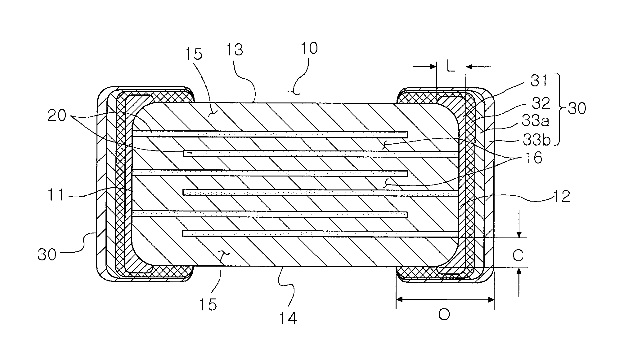
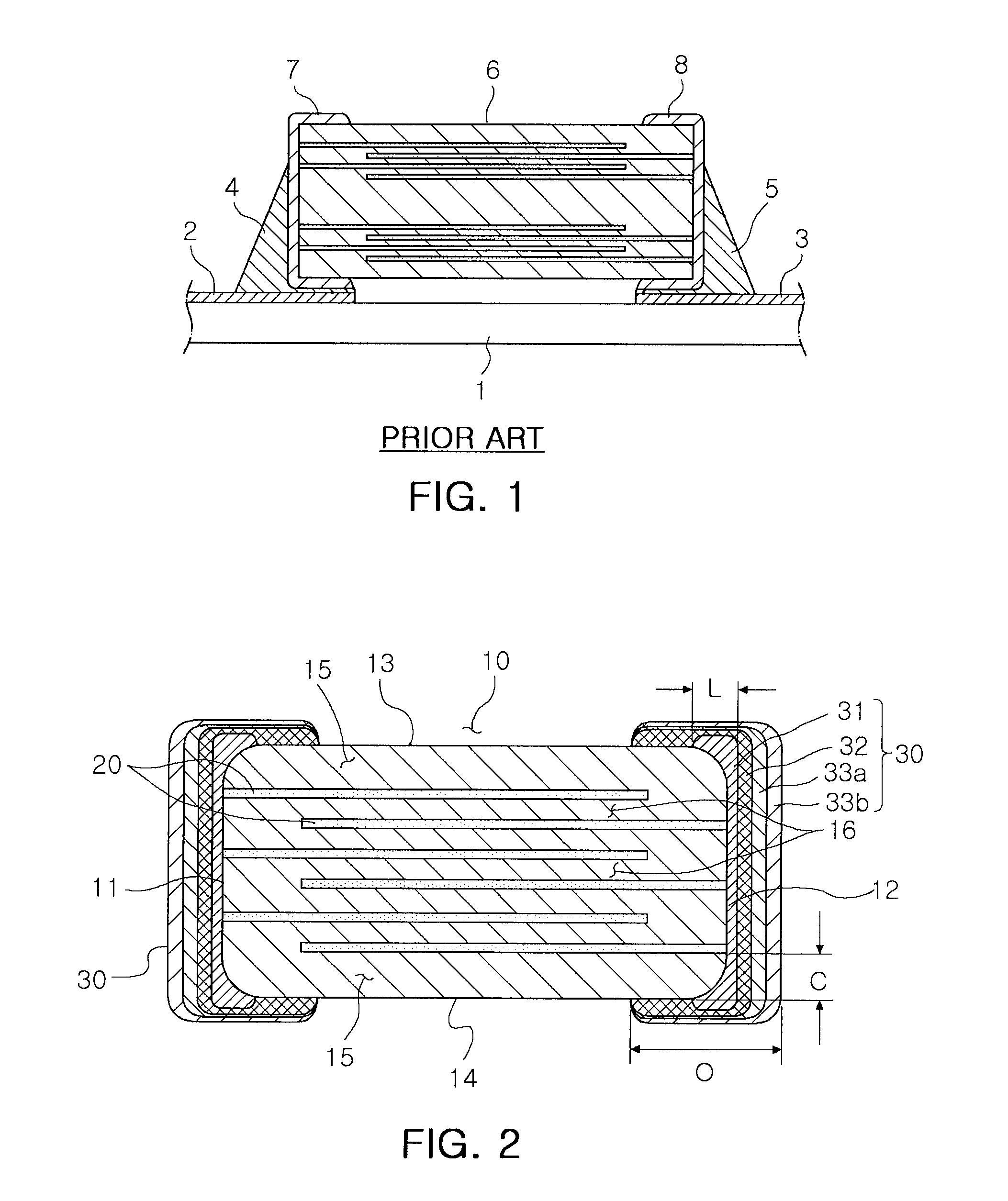
[0060]Ceramic powder having BaTiO3 as its main ingredient and a binder were mixed to form a slurry, and then ceramic green sheets were manufactured by the use of a doctor blade method. A conductive paste having Ni as its main ingredient was applied to the manufactured ceramic green sheets by the use of a screen printing method such that internal electrode patterns were formed. Fifty layers of internal electrodes were laminated and compressed by heat, thereby forming an MLCC laminate. This MLCC laminate was then cut to be 1.6 mm×0.8 mm and fired at 1250° C. in an N2—H2 atmosphere, thereby manufacturing a ceramic sintered body of the MLCC. A conductive paste including glass frit was dipped and coated from the side surfaces of the ceramic sintered body to portions of the top and bottom surfaces thereof such that a pair of first electrode layers were formed. The pair of first electrode layers were fired at 780° C. in a nitrogen atmosphere to be electrically and...


PUM

PropertyMeasurementUnit
Fractionaaaaaaaaaa
Fractionaaaaaaaaaa
Lengthaaaaaaaaaa

Abstract

There is provided a ceramic electronic component including a ceramic sintered body, internal conductive layers, and external electrodes. Each of the external electrodes includes a first electrode layer, a conductive resin layer covering the first electrode layer, and a second electrode layer covering the conductive resin layer and having an extension length greater than the length of the first electrode layer extending from one of the side surfaces of the ceramic sintered body to the portions of the top and bottom surfaces thereof. The distance from the top or bottom surface of the ceramic sintered body to the closest layer of the internal conductive layers is greater than or equal to the length of the first electrode layer extending from one of the side surfaces of the ceramic sintered body to the portions of the top and bottom surfaces thereof.

Description

CROSS-REFERENCE TO RELATED APPLICATIONS[0001]This application claims the priority of Korean Patent Application No. 10-2009-0062591 filed on Jul. 9, 2009, in the Korean Intellectual Property Office, the disclosure of which is incorporated herein by reference.BACKGROUND OF THE INVENTION[0002]1. Field of the Invention[0003]The present invention relates to ceramic electronic components, and more particularly, to ceramic electronic components having a high level of reliability in terms of thermal shock resistance and flexural strength.[0004]2. Description of the Related Art[0005]In general, electronic components using ceramic materials, such as capacitors, inductors, piezoelectric devices, varistors, or thermistors, include a ceramic sintered body made of ceramic materials, internal electrodes formed inside the ceramic sintered body, and external electrodes formed on the surfaces of the ceramic sintered body to be connected to the internal electrodes.[0006]A multi-layer chip capacitor (h...

Claims


Application Information

Patent Timeline
IPC IPC(8): H01G4/12
CPCH01G4/30H01G4/232H01G4/005
Inventor SEO, DONG HWANHUR, KANG HEONKIM, DOO YOUNG
Owner SAMSUNG ELECTRO MECHANICS CO LTD
Why Eureka
Try Eureka