Silicon Carrier Structure and Method of Forming Same

a silicon carrier and silicon technology, applied in the field of electronic systems, can solve the problems of large die size, drive semiconductor die cost up, and inability to process multiple complex mixed logic and memory devices on one wafer, and achieve low cost, high yield, and robust results.

Inactive Publication Date: 2011-01-27
GLOBALFOUNDRIES INC
View PDF11 Cites 24 Cited by
  • Summary
  • Abstract
  • Description
  • Claims
  • Application Information

AI Technical Summary

Benefits of technology

[0015]According to an exemplary embodiment of the present invention, a method of forming a silicon carrier structure includes etching a wafer to form etched vertical holes in the wafer, forming via insulation and metallization using thermal oxidation, forming back-end-of-line wiring to form X-Y wiring interconnections for space transformation connections, power and ground, forming at least one of surface pads, microbumps or copper interconnections, and dicing the wafer to produce one or more silicon carrier structures.
[0016]The present invention will become readily apparent to those of ordinary skill in the art when descriptions of exemplary embodiments thereof are read with reference to the accompanying drawings.

Problems solved by technology

SoC implementations can result in large die sizes and drive semiconductor die costs up due to additional process steps and complexity.
The ability to process multiple complex mixed logic and memory devices as well as other technologies on one wafer may not lead to a robust, high-yield, and low-cost product due to, for example, the complexity of each function not being common with other circuitry or unique processes to obtain system-level functionality.
The gap between processor speeds and memory performance, sometimes referred to as the “memory wall” problem, has become an obstacle to improved computer system performance.
One reason for this difficulty is that the memory system resides “off-chip” and packaging constraints limit what can be accomplished to improve the average time to access memory.
This approach has the disadvantage that the processor die becomes large and therefore expensive.
Bandwidth is one bottleneck in the performance of a memory system.
This method provides means for microwave transmission between moat regions with active devices and high resistivity regions surrounding each moat region on the semiconductor device but does not provide for modular design (reuse of prior designs), lower power or improved performance at lower cost for system level applications.
In these methods for producing chip-stacks, 3D integration of die is typically limited to memory products including Flash, SRAM and DRAM, which are edge wire-bonded.
These methods do not address the memory bottleneck.

Method used


Image

  • Silicon Carrier Structure and Method of Forming Same
  • Silicon Carrier Structure and Method of Forming Same
  • Silicon Carrier Structure and Method of Forming Same

Examples


Embodiment Construction

[0021]Hereinafter, exemplary embodiments of the present invention will be described with reference to the accompanying drawings.

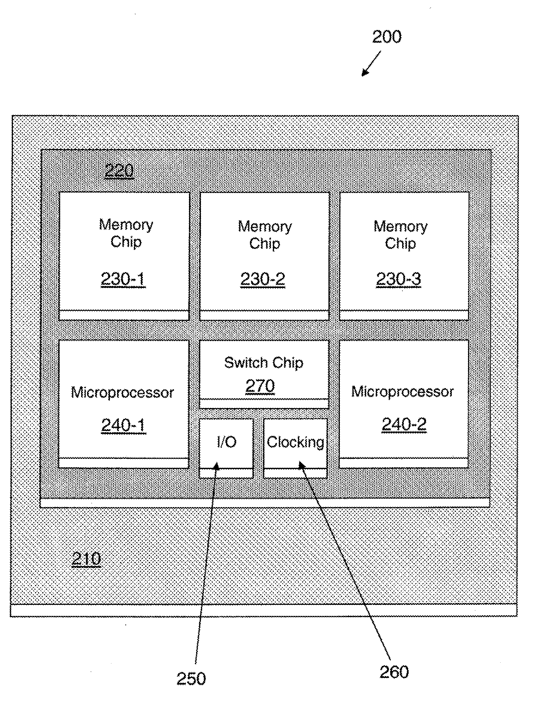
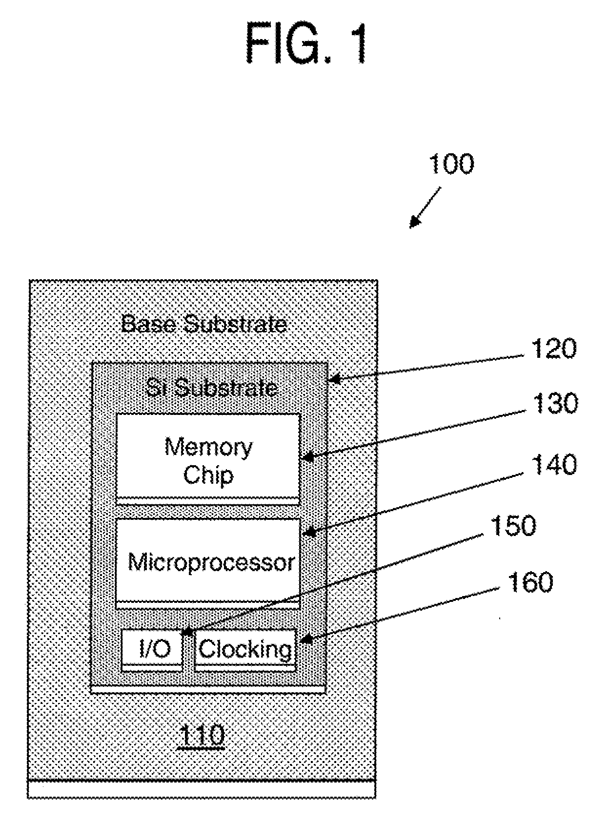
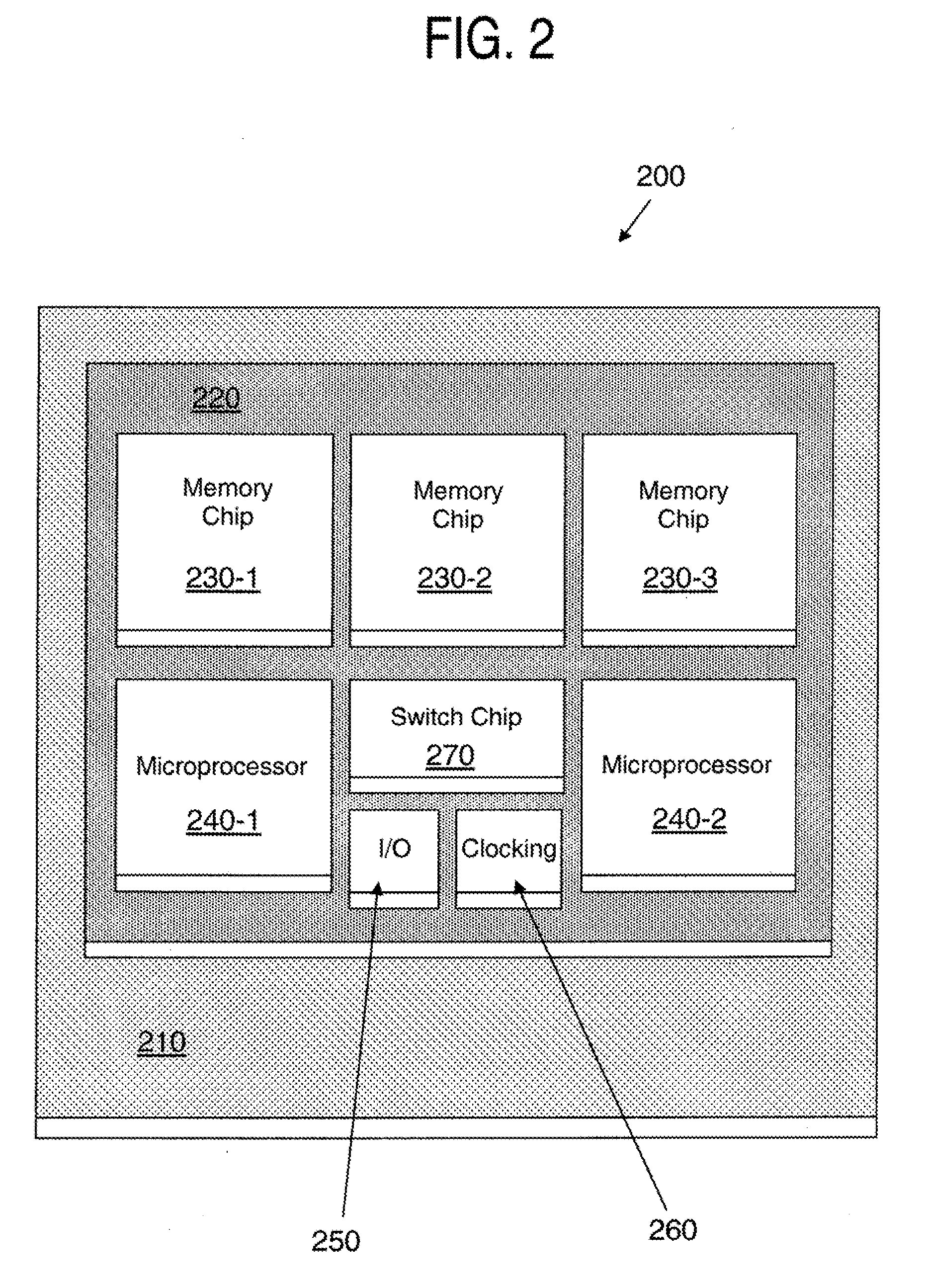
[0022]Various exemplary embodiments of the present invention include a surface mountable integrated circuit fabricated in a silicon carrier or wafer with interconnection to silicon chips or connection with a printed circuit board as well as a structure and method for high-performance electronic packaging assembly using a silicon interposer to connect microprocessor and memory chips.

[0023]A silicon carrier structure, according to an exemplary embodiment of the present invention, includes flip-chips attached without the use of engineering pad changes between the semiconductor devices, creating a shorter path for interconnection and permitting testing and changes on the opposite side of the substrate, and permitting reduced length connections. Further, top surface repair may be substantially avoided.

[0024]Various exemplary embodiments of the present invention ...


PUM

PropertyMeasurementUnit
diameteraaaaaaaaaa
diameteraaaaaaaaaa
heightaaaaaaaaaa

Abstract

A silicon carrier structure for electronic packaging includes a base substrate, a silicon carrier substrate disposed on the base substrate, a memory chip disposed on the silicon carrier substrate, a microprocessor chip disposed on the silicon carrier substrate, an input/output chip disposed on the silicon carrier substrate, and a clocking chip disposed on the silicon carrier substrate.

Description

BACKGROUND OF THE INVENTION[0001]1. Technical Field[0002]The present disclosure relates to electronic systems and, more particularly, to packaging of electronic systems.[0003]2. Discussion of Related Art[0004]In the computer industry, packaging methods include building circuits forming a system on a single die, referred to as a SoC (System on Chip) device, building circuits forming a system on two or more chips according to chip device type, or packaging each chip into an electronic package and later assembling them on an organic substrate or a printed circuit board (PCB). Chips, such as SoC devices, may be used for high-performance computing solutions or complex combined technology solutions. SoC implementations can result in large die sizes and drive semiconductor die costs up due to additional process steps and complexity. The ability to process multiple complex mixed logic and memory devices as well as other technologies on one wafer may not lead to a robust, high-yield, and low...

Claims


Application Information

Patent Timeline
Patent Type & Authority Applications(United States)
IPC IPC(8): H05K1/18C23F1/00
CPCH01L23/147H01L23/60H01L25/0652H01L25/0655H01L2924/157H01L2924/10253H01L2224/16225Y02T10/82H01L2924/00
Inventor ANDRY, PAUL STEPHENHOFSTEE, HARM PETERKATOPIS, GEORGE A.KNICKERBOCKER, JOHN ULRICHMONTOYE, ROBERT K.PATEL, CHIRAG S.
Owner GLOBALFOUNDRIES INC
Why Eureka
Try Eureka