Double-gate floating-body memory device

a floating-body memory and double-gate technology, applied in the field of memory devices, can solve the problems of insufficient supply voltage requirements, difficulty in reducing the overall size of the memory or increasing the capacity of the memory, and difficulty in reducing the size of each memory cell, so as to achieve the effect of increasing the spacing

Inactive Publication Date: 2011-01-27
CENT NAT DE LA RECHERCHE SCI
View PDF13 Cites 14 Cited by
  • Summary
  • Abstract
  • Description
  • Claims
  • Application Information

AI Technical Summary

Benefits of technology

[0016]In an embodiment of the present invention, the method comprises increasing the spacing between the source and drain regions and the second gate electrode by performing, after formation of the insulating layer in oxide and of the gate electrode of the first gate, an oxidization step such the oxide thickness at ends of the insulating layer in the areas of the source and drain regions is increased.
[0017]An embodiment of the present invention also provides a method of operating a memory device comprising a transistor having a floating body positioned between source and drain regions, the floating body being sandwiched between first and second gates each comprising a gate electrode and an insulating layer positioned between the floating body and the gate electrode, the method comprising applying one of first and second voltage level between the gate electrode of the first gate and at least one of the source and drain regions to program the state of said floating body to have an accumulation or depletion of majority carriers; and applying a third voltage level to the gate electrode of the second gate to retain the programmed state of said floating body.

Problems solved by technology

A problem with such DRAM devices is that the capacitor is bulky and therefore it is very difficult to reduce the size of each memory cell and thus reduce the overall size of the memory or increase its capacity.
However, the solutions that have been proposed until now are generally inadequate in terms of the retention time of each memory cell, the supply voltage requirements for writing, holding or reading data, and / or the ability of the memory cells to be used in an array.

Method used


Image

  • Double-gate floating-body memory device
  • Double-gate floating-body memory device
  • Double-gate floating-body memory device

Examples


Embodiment Construction

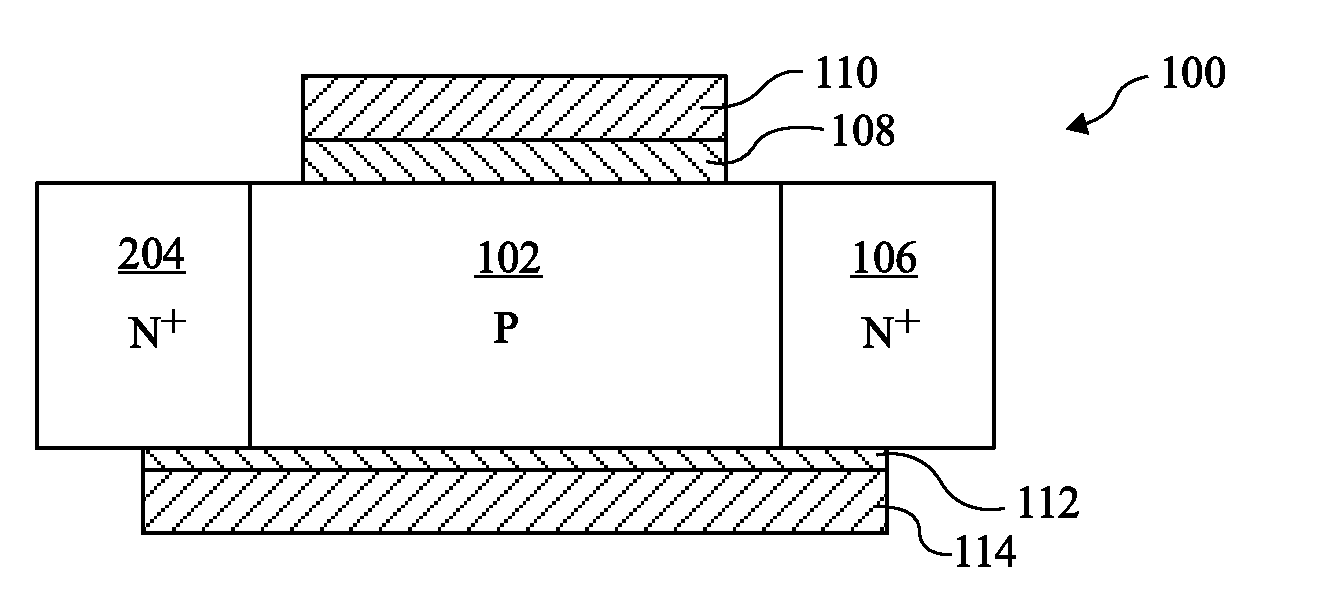
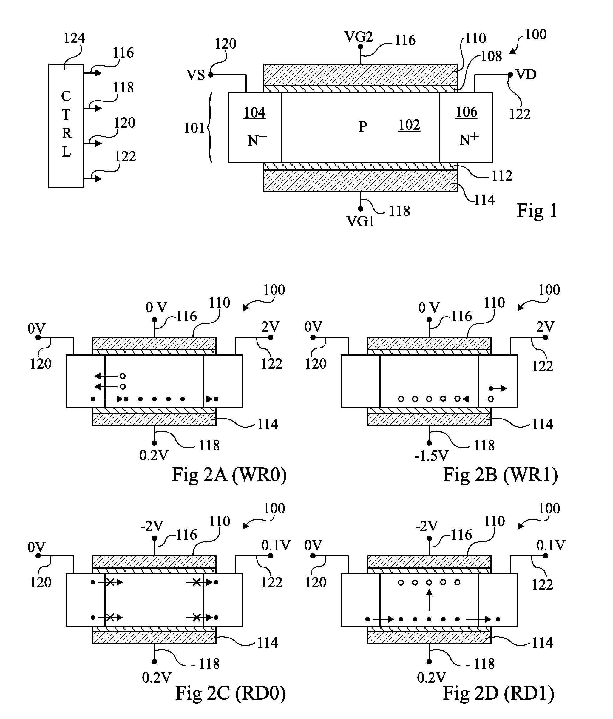
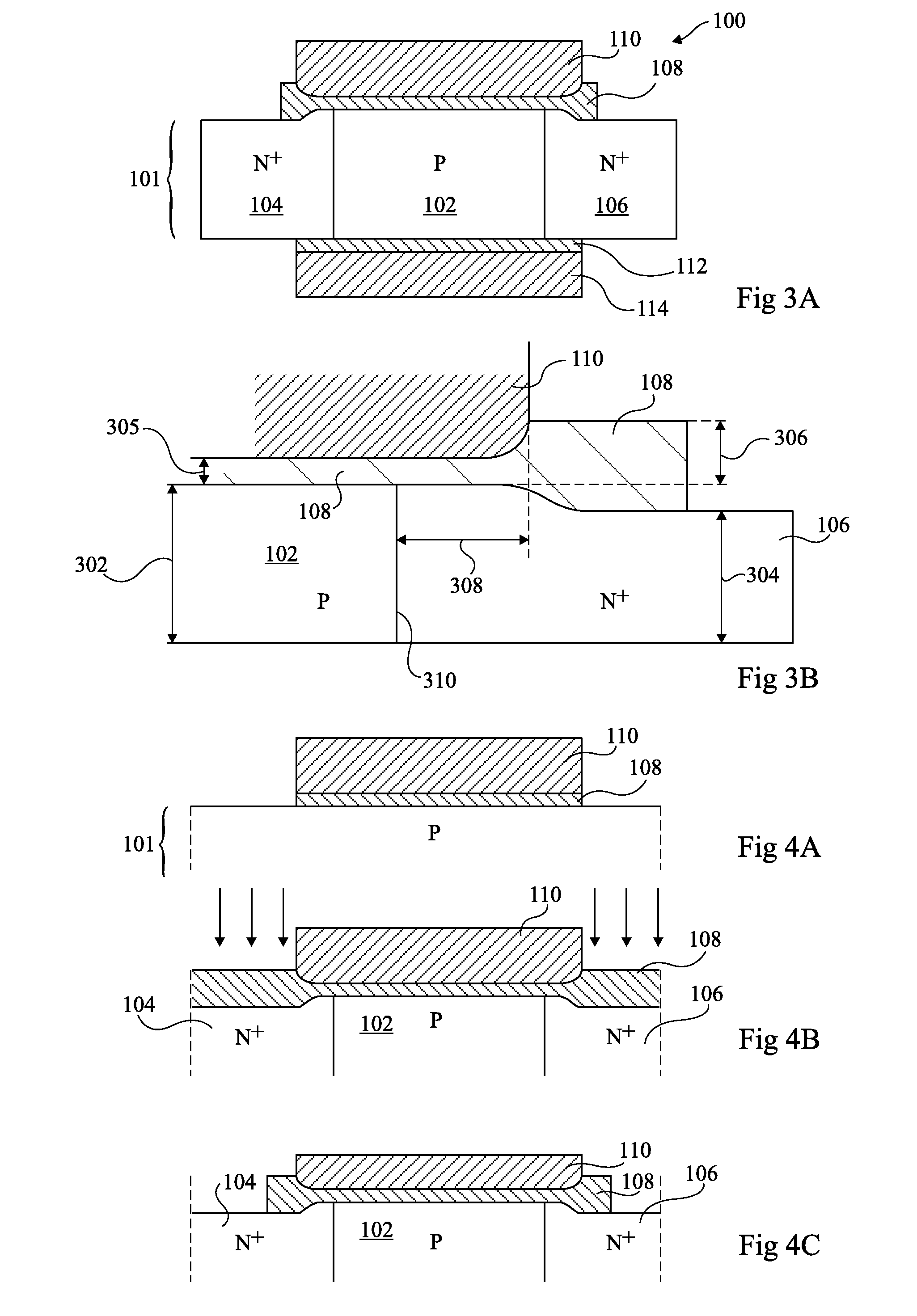
[0029]FIG. 1 schematically illustrates in cross-section a memory device 100, comprising a thin silicon film 101 sandwiched between two opposing gates. The thin silicon film 101 comprises a P-type floating body 102 positioned between N-type source and drain regions 104 and 106 respectively.

[0030]The top gate in FIG. 1 is formed on the top side of the thin silicon film 101 and comprises an insulating layer 108 separating the body 102 from a gate electrode 110, which is for example formed of polysilicon or another conducting material. The bottom gate in FIG. 1 is formed on the opposite side of the thin silicon film 101 and comprises an insulating layer 112 separating the body from a gate electrode 114.

[0031]Gate contacts 116 and 118 make electrical contact with the gate electrodes 110 and 114 respectively. A source contact 120 makes contact with the source region 104, while a drain contact 122 makes contact with the drain region 106.

[0032]The thin silicon film 101 for example has a thi...


PUM


Abstract

A memory device is provided comprising a transistor having a floating body positioned between source and drain regions, the floating body being sandwiched between first and second insulated gates each comprising a gate electrode. A control circuit is arranged to program the state of said floating body to have an accumulation or depletion of majority carriers by applying one of first and second voltage levels between the first gate and at least one of the source and drain regions, and to retain the programmed state of said floating body by applying a third voltage level to the second gate. The voltages are switched over a time duration shorter than 100 ns.

Description

FIELD OF THE INVENTION[0001]The present invention relates to a memory device comprising two gates and a floating body, to a method of controlling such a memory device and to a memory comprising an array of such memory devices.BACKGROUND OF THE INVENTION[0002]DRAMs (dynamic random access memories) comprise an array of memory cells, each memory cell generally comprising a transistor and a capacitor. One bit of data is memorized by each cell by storing, via the transistor, a level of electrical charge on the capacitor. The stored data is refreshed periodically.[0003]A problem with such DRAM devices is that the capacitor is bulky and therefore it is very difficult to reduce the size of each memory cell and thus reduce the overall size of the memory or increase its capacity.[0004]To solve this problem, alternative memory structures have been proposed, in which a memory cell comprises just a single transistor having a floating body. Thus rather than storing charge on a capacitor, charge i...

Claims


Application Information

Patent Timeline
Patent Type & Authority Applications(United States)
IPC IPC(8): G11C7/22H01L21/336
CPCG11C11/404G11C11/4085H01L29/7841H01L27/108H01L27/10802G11C2211/4016H10B12/20H10B12/00
Inventor BAWEDIN, MARYLINECRISTOLOVEANU, SORIN IOANFLANDRE, DENISRENAUX, CHRISTIANCRAHAY, ANDRE
Owner CENT NAT DE LA RECHERCHE SCI
Why Eureka
Try Eureka