Semiconductor device and method of manufacturing the same
- Summary
- Abstract
- Description
- Claims
- Application Information
AI Technical Summary
Benefits of technology
Problems solved by technology
Method used
Image

Examples
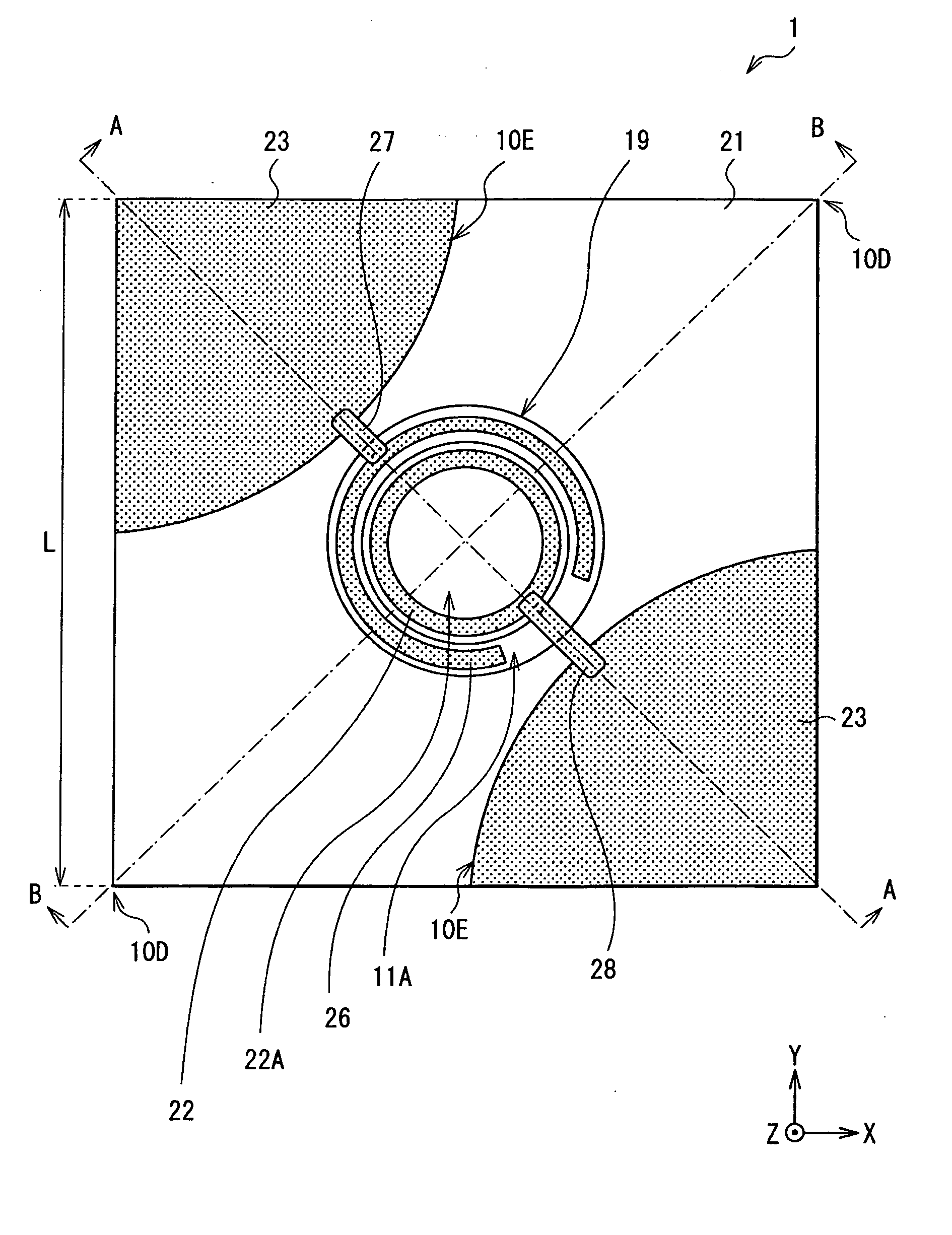
first embodiment
Modification of First Embodiment
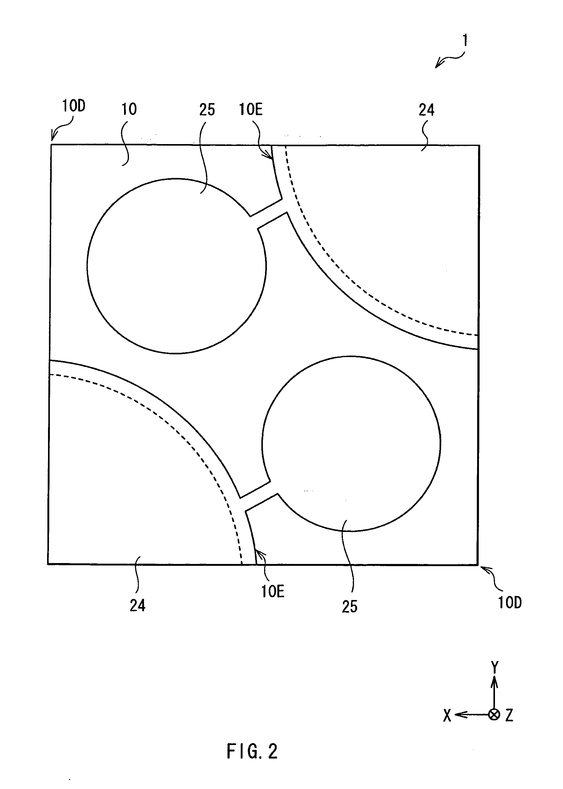
[0081]Although the notch 10E is formed at a corner of the chip in the embodiment, for example, as illustrated in FIGS. 11 and 12, it may be formed in a side of the chip. In such a case, in the manufacturing process, for example, as illustrated in FIGS. 13 and 14, it is sufficient to form the metal layers 23D and 24D over a part except for the intersection 10× in the cutting region 10F.
Second Embodiment
[0082]A vertical cavity surface laser diode 2 according to a second embodiment of the present invention will now be described. FIG. 15 is a top view of the laser diode 2. FIG. 16 is a back side view of the laser diode 2 of FIG. 15. FIG. 17 illustrates a sectional configuration taken along line A-A of the laser diode 2 of FIG. 15. FIG. 18 illustrates a sectional configuration taken along line B-B of the laser diode 2 of FIG. 15.
[0083]Like the laser diode 1 of the foregoing embodiment, the laser diode 2 is a chip having a structure suitable for flip chip b...
second embodiment
Modification of Second Embodiment
[0096]Although the notch 10E is formed at a corner of the chip in the second embodiment, for example, like in the modification of the first embodiment, it may be formed in a side of the chip.
[0097]In place of lapping the under face 10B of the substrate 10 after formation of the connection parts 27 and 28 in the manufacturing process of the second embodiment, another process may be performed. For example, by etching all or selectively etching a part of the region opposed to the bottom face of the dent 50 in the under face 10B of the substrate 10, the face on the bottom face side of the dent 50 in the metal layer 23D may be exposed.
[0098]Although the present invention has been described by the embodiments and their modifications, the invention is not limited to the embodiments but may be variously modified.
[0099]For example, although the present invention has been described using a vertical cavity surface laser diode as an example in the foregoing embo...
PUM
 Abstract
Description
Claims
Application Information