Semiconductor laser device

Active Publication Date: 2012-06-14
ROHM CO LTD
View PDF2 Cites 2 Cited by
  • Summary
  • Abstract
  • Description
  • Claims
  • Application Information

AI Technical Summary

Benefits of technology

[0008]In order to maintain compatibility with the existing sliding contactor manufacturing step in the “thermally assisted record” manner, a semiconductor laser device use

Problems solved by technology

Moreover, a mounting space of a semiconductor laser device is limited, and due to different optical system designs, sometimes not only general Transverse Elect

Method used


Image

  • Semiconductor laser device
  • Semiconductor laser device
  • Semiconductor laser device

Examples


Example

[0048]Below, implementation manners of the present invention are illustrated in detail with reference to accompanying drawings.

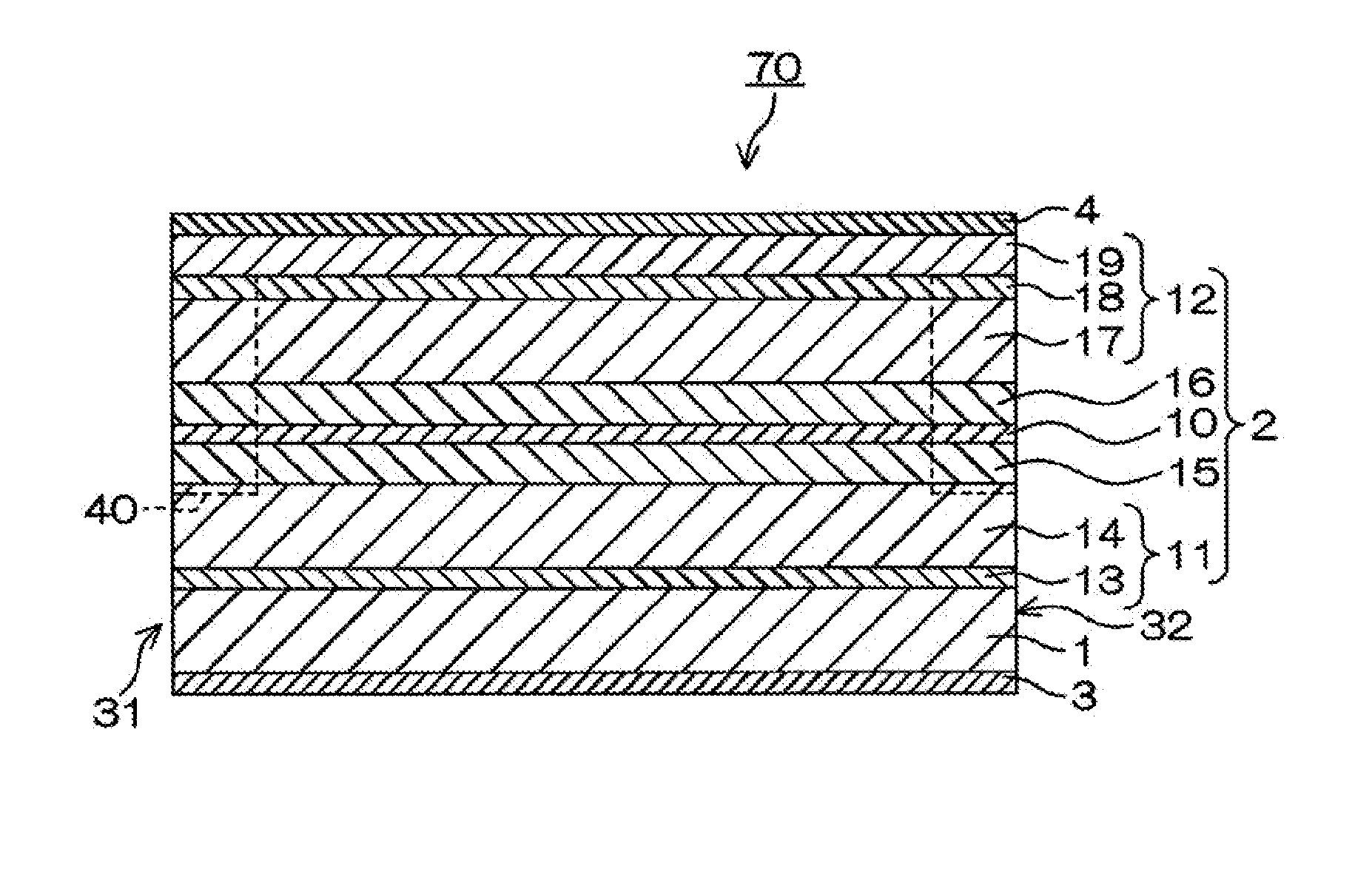
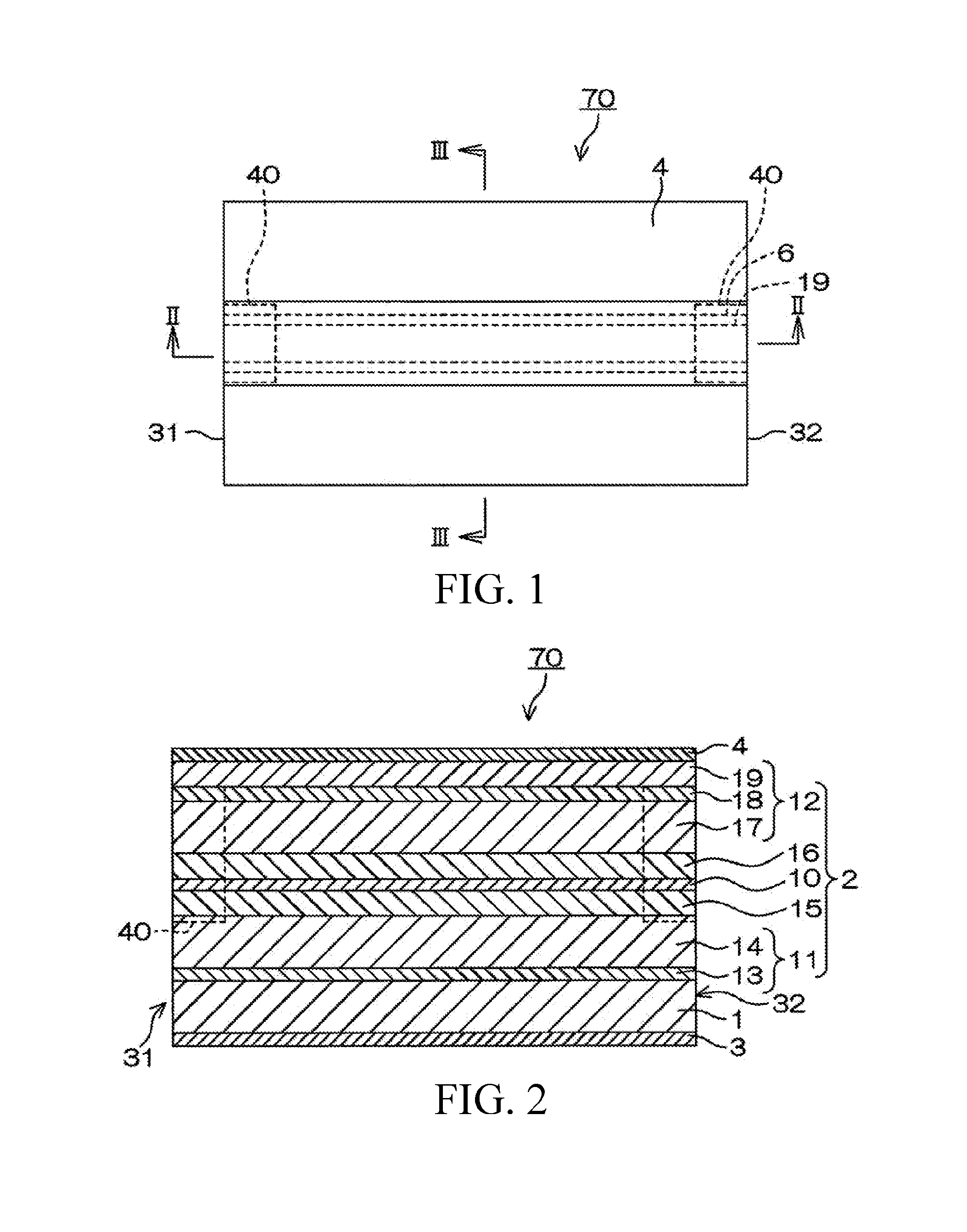
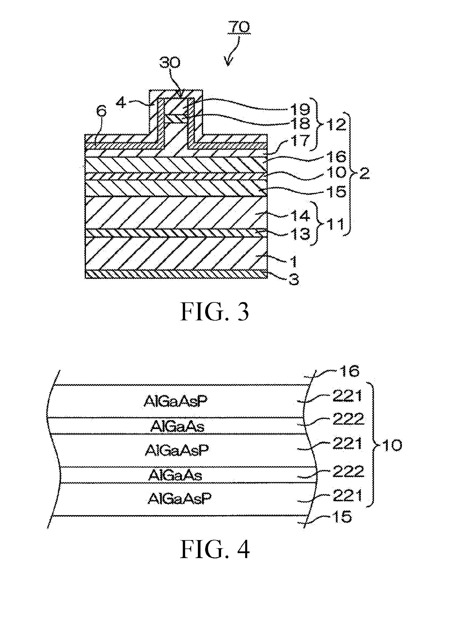
[0049]FIG. 1 is a top view used to illustrate a structure of a semiconductor laser diode according to an implementation manner of the present invention, FIG. 2 is a sectional view along line II-II in FIG. 1, and FIG. 3 is a sectional view along line III-III in FIG. 1.

[0050]The semiconductor laser diode 70 is of a Fabry-Perot type that includes: a substrate 1; a semiconductor stacked structure 2, which is formed on the substrate 1 through crystal growth; an n-type electrode 3, which is formed in a manner of contacting the back of the substrate (a surface opposite to the semiconductor stacked structure 2); and a p-type electrode 4, which is formed in a manner of contacting a surface of the semiconductor stacked structure 2.

[0051]The substrate 1 is formed of a GaAs monocrystalline substrate in the implementation manner. The face orientation of the surface of th...


PUM


Abstract

A semiconductor laser device capable of high output is provided. A semiconductor laser diode includes: a substrate; and a semiconductor stacked structure, which is formed on the substrate through crystal growth. The semiconductor stacked structure includes: an n-type (Alx1Ga(1-x1))0.51In0.49P cladding layer 14 and a p-type (Alx1Ga(1-x1))0.51In0.49P cladding layer; an n-side Alx2Ga(1-x2)As guiding layer and a p-side Alx2Ga(1-x2)As guiding layer, which are sandwiched between the cladding layers; and an active layer, which is sandwiched between the guiding layers. The active layer is formed of a quantum well layer including an AlyGa(1-y)As(1-x3)Px3 layer and a barrier layer including an Alx4Ga(1-x4)As layer that are alternatively repetitively stacked for a plurality of periods.

Description

BACKGROUND OF THE INVENTION[0001]1. Field of the Invention[0002]The present invention relates to a semiconductor laser device.[0003]2. Description of the Related Art[0004]In order to increase storage capacity of a hard disc apparatus (HDD: Hard disc Drive), it is required to write a signal to a micro area of a magnetic disc. In order to both ensure the thermal stability of the signal and the recording of the signal in the micro area, a record medium with thermal stability is required, but the problem that overwriting needs a strong magnetic field will be generated. Currently, in an existing Giant Magneto Resistance (GMR) manner, record density tends to be saturated; therefore it is intended to achieve a “thermally assisted record” manner. The “thermally assisted record” manner is a manner in which a laser diode (semiconductor laser device) is used as a heat source to temporarily alleviate a force maintaining by a magnetic field and perform the task of writing.DOCUMENT IN THE PRIOR A...

Claims


Application Information

Patent Timeline
IPC IPC(8): H01S5/343
CPCB82Y20/00H01S5/2031H01S5/22H01S5/3202H01S5/3436H01S5/3404H01S5/3434H01S2301/145H01S2301/173H01S5/3213
Inventor NOMA, TSUGUKIAKUTSU, MINORUNISHIOKA, YOSHITO
Owner ROHM CO LTD
Why Eureka
Try Eureka