Printed circuit board and method of fabricating the same

a technology of printed circuit board and insulating layer, which is applied in the direction of printed circuit aspects, printed circuit non-printed electric components association, conductive pattern formation, etc., can solve the problems of undesirably prolonging lead time, deteriorating the reliability of pcb, and undesirably separation of circuit layer, so as to reduce lead time and fabrication cost, and minimize the separation of circuit layer

Inactive Publication Date: 2011-02-03
SAMSUNG ELECTRO MECHANICS CO LTD
View PDF2 Cites 16 Cited by
  • Summary
  • Abstract
  • Description
  • Claims
  • Application Information

AI Technical Summary

Benefits of technology

[0023]Accordingly, the present invention has been made keeping in mind the problems encountered in the related art and the present invention intends to provide a PCB and a method of fabricating the same, in which the PCB is fabricated using a build-up process and the outermost circuit layer thereof is formed to have an embedded structure using a simple imprinting process, thus minimizing the separation of the circuit layer and reducing the lead time and the fabrication cost.

Problems solved by technology

However, because the circuit pattern 28 resulting from the conventional semi-additive process is provided in the form of a positive pattern on the insulating layer 12, it may be undesirably separated from the insulating layer 12.
In a multilayered PCB, the separation of the circuit pattern 28 formed on the outermost layer drastically deteriorates the reliability of the PCB.
However, in order to reduce plating deviation occurring between the region having the trench 56 and the region having no trench, an additional polishing process should be performed, and also, trench processing and polishing should be conducted in respective layers, undesirably prolonging the lead time.
Furthermore, because equipment used in the formation of the trench is expensive, the fabrication cost is undesirably increased.
Therefore, it is difficult to fabricate the multilayered PCB using only LPP.

Method used


Image

  • Printed circuit board and method of fabricating the same
  • Printed circuit board and method of fabricating the same
  • Printed circuit board and method of fabricating the same

Examples


first embodiment

[0052]FIG. 11 is a cross-sectional view showing a PCB according to the present invention. With reference to this drawing, the PCB 100a according to the present embodiment is described below.

[0053]As shown in FIG. 11, the PCB 100a according to the present embodiment includes an insulating member 120 having a circuit pattern 130 embedded in one surface thereof, a build-up layer 140 formed on the insulating member 120 and including a build-up insulating layer 142 and a circuit layer 144, and a solder resist layer 150 formed on the build-up layer 140.

[0054]The circuit pattern 130 is embedded in one surface of the insulating member 120, and specifically, is embedded to be flush with one surface of the insulating member 120. As such, the circuit pattern 130 is formed only in a portion of one surface of the insulating member 120 in a thickness direction. To this end, a pattern trench 122 is formed through an imprinting process and is then subjected to plating, so that the circuit pattern 1...

second embodiment

[0058]FIG. 12 is a cross-sectional view showing a PCB according to the present invention. With reference to this drawing, the PCB 100b according to the present embodiment is described below.

[0059]As shown in FIG. 12, the PCB 100b according to the present embodiment has the same configuration as that of the PCB according to the first embodiment, with the exception that bump pads 132 are formed to be exposed to the other surface of an insulating member 120 while being connected to a circuit pattern 130 embedded in one surface of the insulating member 120. The redundant descriptions for the same elements are omitted.

[0060]The bump pads 132 are formed to be flush with the other surface of the insulating member 120, and thus have a surface exposed to the other surface of the insulating member 120. Unlike the PCB 100a according to the first embodiment, in the PCB 100b according to the present embodiment, because the bump pads 132 connected to the circuit pattern 130 are formed to extend t...

third embodiment

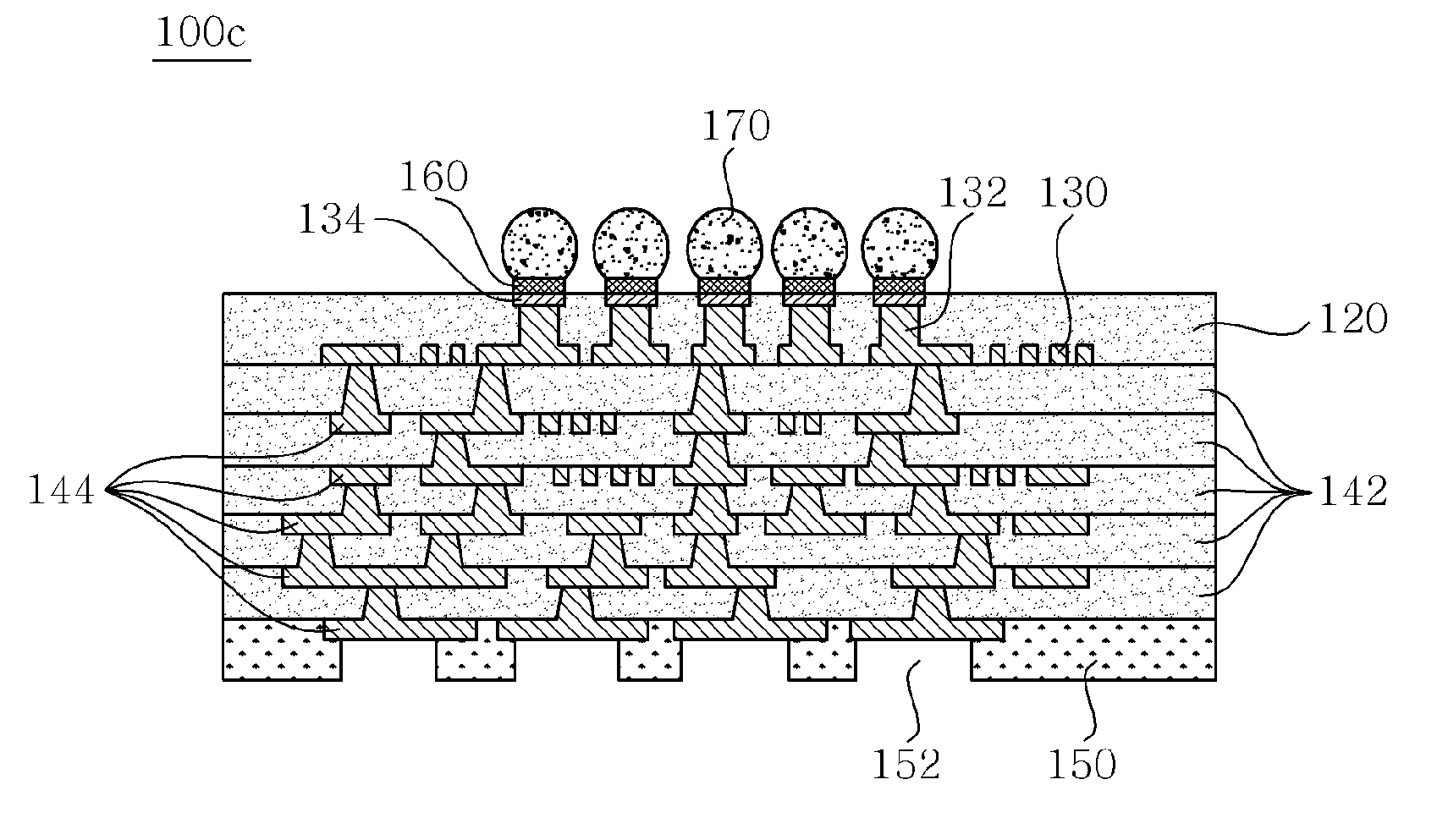
[0061]FIG. 13 is a cross-sectional view showing a PCB according to the present invention. With reference to this drawing, the PCB 100c according to the present embodiment is described below.

[0062]As shown in FIG. 13, the PCB 100c according to the present embodiment is configured such that recesses are processed in portions of the bump pads 132 positioned at the other surface of the insulating member 120 and a portion of the insulating member 120 around the portions of the bump pads 132 in the PCB 100b according the second embodiment, and thus assistant pads 134 connected to the bump pads 132 are formed in the recesses. Specifically, the assistant pads 134 which have a diameter greater than that of the bump pads 132 and are flush with the other surface of the insulating member 120 are provided, whereby the contact area thereof with the external connection terminals 170 is enlarged, thus enhancing adhesivity to the external connection terminals 170. As such, a surface treatment layer ...


PUM

PropertyMeasurementUnit
thicknessaaaaaaaaaa
diameteraaaaaaaaaa
thicknessaaaaaaaaaa

Abstract

Disclosed is a printed circuit board, which includes an insulating member having a circuit pattern embedded in one surface thereof, a build-up layer formed on one surface of the insulating member and including a build-up insulating layer and a circuit layer formed in the build-up insulating layer and having a via connected to the circuit pattern, and a solder resist layer formed on the build-up layer. A method of fabricating the printed circuit board is also provided. The printed circuit board is fabricated using a build-up process and the outermost circuit layer thereof is formed to have an embedded structure using an imprinting process, thus minimizing the separation of the circuit layer and reducing the lead time and the fabrication cost.

Description

CROSS REFERENCE TO RELATED APPLICATION[0001]This application claims the benefit of Korean Patent Application No. 10-2009-0070634, filed Jul. 31, 2009, entitled “A printed circuit board and a fabricating method the same”, which is hereby incorporated by reference in its entirety into this application.BACKGROUND OF THE INVENTION[0002]1. Technical Field[0003]The present invention relates to a printed circuit board (PCB) and a method of fabricating the same.[0004]2. Description of the Related Art[0005]Recently, in order to cope with an increase both in signal transmission speed and density of a semiconductor chip, the demand for techniques for directly mounting a semiconductor chip on a PCB is increasing. Thus, the development of a PCB having high density and high reliability capable of coping with the increase in the density of the semiconductor chip is required.[0006]The requirements for the PCB having high density and high reliability are closely related to the specs of the semicondu...

Claims


Application Information

Patent Timeline
Patent Type & Authority Applications(United States)
IPC IPC(8): H05K1/11H05K3/10
CPCH01L21/4857Y10T29/49147H01L23/49822H01L23/49894H05K3/0097H05K3/045H05K3/4682H05K2201/0376H05K2203/0108H05K2203/0733H01L2924/0002H01L23/49816Y10T29/49155Y10T29/49128H01L2924/00H05K1/02
Inventor KO, YOUNG GWAN
Owner SAMSUNG ELECTRO MECHANICS CO LTD
Why Eureka
Try Eureka