Printed circuit board and method of manufacturing the same

a printed circuit board and manufacturing method technology, applied in the direction of printed circuit aspects, non-metallic protective coating applications, conductive pattern formation, etc., can solve the problems of reducing the reliability of printed circuit boards, increasing manufacturing costs, and prolonging lead time, so as to achieve simple performance and minimize the separation of circuit layers

Active Publication Date: 2011-04-21
SAMSUNG ELECTRO MECHANICS CO LTD
View PDF7 Cites 12 Cited by
  • Summary
  • Abstract
  • Description
  • Claims
  • Application Information

AI Technical Summary

Benefits of technology

[0021]Accordingly, the present invention has been made keeping in mind the problems encountered in the related art and the present invention is intended to provide a printed circuit board, which is constructed in a build-up manner and which includes an outermost layer having an embedded structure obtained through an imprinting technology which is simply performable, thus minimizing separation of a circuit layer, and a method of manufacturing the same.

Problems solved by technology

In a multilayered printed circuit board, the separation of the circuit pattern formed on the outermost layer seriously decreases reliability of the printed circuit board.
However, LPP requires an additional grinding process in order to reduce a difference in plating thicknesses between a region with the trenches 18a and 19a and a region without the trenches, and a process of forming the trenches 18a and 19a and a grinding process must be executed at every layer, thus causing extension of lead time.
In addition, since process machinery which is used in the formation of the trenches 18a and 19a is expensive, manufacturing costs are correspondingly increased.
Furthermore, although it is also possible to form a fine circuit by forming trenches using an imprint process, the interlayer alignment significantly deteriorates, thus precluding application to a build-up board.

Method used


Image

  • Printed circuit board and method of manufacturing the same
  • Printed circuit board and method of manufacturing the same
  • Printed circuit board and method of manufacturing the same

Examples


first embodiment

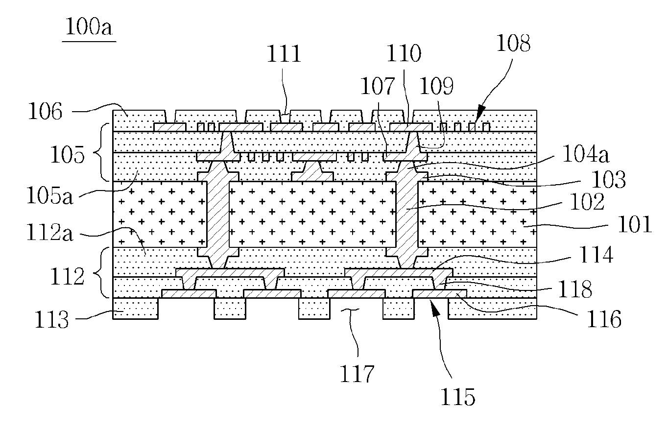
[0054]FIG. 8 is a cross-sectional view of a printed circuit board 100a according to the present invention. With reference to the drawing, the printed circuit board 100a according to this embodiment of the invention is described below.

[0055]As shown in FIG. 8, the printed circuit board 100a according to this embodiment is configured such that a core substrate 101, which has through-hole parts 102 and core circuit layers 103 formed on both sides thereof, is provided on one side thereof with a first build-up layer 105 and a first protective layer 106 and is provided on the other side thereof with a second build-up layer 112 and a second protective layer 113, and the outermost circuit layer of the first build-up layer 105 is embodied as a trench circuit layer 108 that is formed using a trench technology.

[0056]Although each of the first build-up layer 105 and the second build-up layer 112 is shown in FIG. 8 as being composed of two layers, it is provided only for illustrative purposes an...

second embodiment

[0076]The bumps 104a may be formed by a metal plating layer or electroconductive metal paste. In this embodiment, the bumps 104a are described as being formed by a metal plating layer, and are described as being formed by electroconductive metal paste in a

[0077]The bumps 104a are provided for forming the electrical connection between the core circuit layer 103 and the innermost circuit layer 107 of the first build-up layer 105 (to be described later) as well as for the electrical connection between the core circuit layer 103 and the innermost circuit layer 114 of the second build-up layer 112. The bumps 104a are configured to protrude from the circuit layer 103. The bumps 104a may be integrally formed along with the core circuit layers 103 by executing a plating process once, or may be separately formed by executing a plating process after formation of the core circuit layers 103. The process of forming the bumps 104a is not limited to the above-mentioned processes but may be formed...


PUM

PropertyMeasurementUnit
critical thicknessaaaaaaaaaa
electroconductiveaaaaaaaaaa
signal transmission speedaaaaaaaaaa

Abstract

Disclosed are a printed circuit board including a core substrate including core circuit layers on both sides thereof, a first build-up layer formed on one side of the core substrate, a second build-up layer formed on the other side of the core substrate, and first and second protective layers formed on the first and second build-up layers, respectively, wherein the first build-up layer includes a trench circuit layer as an outermost circuit layer formed by a trench technology, the trench circuit layer is embedded in the first protective layer, and an outermost circuit layer of the second build-up layer is embedded in an outermost insulating layer of the second build-up layer, and a method of manufacturing the printed circuit board. Thanks to the formation of the outermost circuit layer by the trench technology, it is difficult to separate the outermost circuit layer from the outermost insulating layer.

Description

CROSS REFERENCE TO RELATED APPLICATION[0001]This application claims the benefit of Korean Patent Application No. 10-2009-0099869, filed Oct. 20, 2009, entitled “A printed circuit board and a fabricating method the same”, which is hereby incorporated by reference in its entirety into this application.BACKGROUND OF THE INVENTION[0002]1. Technical Field[0003]The present invention relates to a printed circuit board and a method of manufacturing the same.[0004]2. Description of the Related Art[0005]Recently, in order to cope with an increase both in signal transmission speed and density of semiconductor chips, the demand for techniques for directly mounting a semiconductor chip on a PCB is increasing. Thus, the development of a PCB having high density and high reliability capable of coping with the increasing density of the semiconductor chip is required.[0006]The requirements for the PCB having high density and high reliability are closely related to the specs of the semiconductor chip,...

Claims


Application Information

Patent Timeline
Patent Type & Authority Applications(United States)
IPC IPC(8): H05K1/11H05K3/10
CPCH05K3/007H05K3/107H05K3/28H05K3/4602H05K3/462Y10T29/49155Y10T29/49144Y10T29/4913Y10T29/49165Y10T29/49126Y10T29/49117H05K2201/09536H05K3/46
Inventor KO, YOUNG GWAN
Owner SAMSUNG ELECTRO MECHANICS CO LTD
Why Eureka
Try Eureka