Inverted Metamorphic Multijunction Solar Cells with Back Contacts

a solar cell and metamorphic technology, applied in the field of semi-conductor-based solar cells, can solve the problems of difficult electrical interconnection through standard bonding of wires, such as kovar® wires, and entail a rather complex manufacturing process, and achieve the effects of less costly, secure and robust electrical interconnection, and convenient performan

Active Publication Date: 2011-02-10
SOLAERO TECH CORP
View PDF89 Cites 44 Cited by
  • Summary
  • Abstract
  • Description
  • Claims
  • Application Information

AI Technical Summary

Benefits of technology

[0014]It is an object of the present invention to provide a back-contact solar cell that can be manufactured with a process that is reliable and easy to perform.
[0015]It is another object of the present invention to provide a solar cell of mesa type having a contact structure connecting the front side with the back side of the cell, which is secure and robust for electrical interconnections.
[0016]It is still another object of the present invention to provide a solar cell of mesa type having a structure of the opposite polarity electrodes, which can be defined with geometries and dimensions such that standard lithography can be used, and, preferably, can be manufactured by using less costly etching processes, such as selective wet chemical etching.
[0017]A further object of the present invention is to provide a reliable and cost-effective method of manufacturing a back-contact solar cell.

Problems solved by technology

The inventors have observed that, in back-contact solar cells, formation of the holes and of the conductive path to bring the front electrode, e.g., the bus bar of the front electrode, to the backside of the cell may entail rather complex manufacturing process, due to an increase of the number of process steps and to constraints in the geometry and dimension of the through-holes.
The inventors have also noted that electrical interconnection by means of standard bonding of wires, such as Kovar® wires, can be problematic because of the fragility of the solar cells, and in particular of the conductive layer electrically connecting the front electrode with the cell's backside.

Method used


Image

  • Inverted Metamorphic Multijunction Solar Cells with Back Contacts
  • Inverted Metamorphic Multijunction Solar Cells with Back Contacts
  • Inverted Metamorphic Multijunction Solar Cells with Back Contacts

Examples


Embodiment Construction

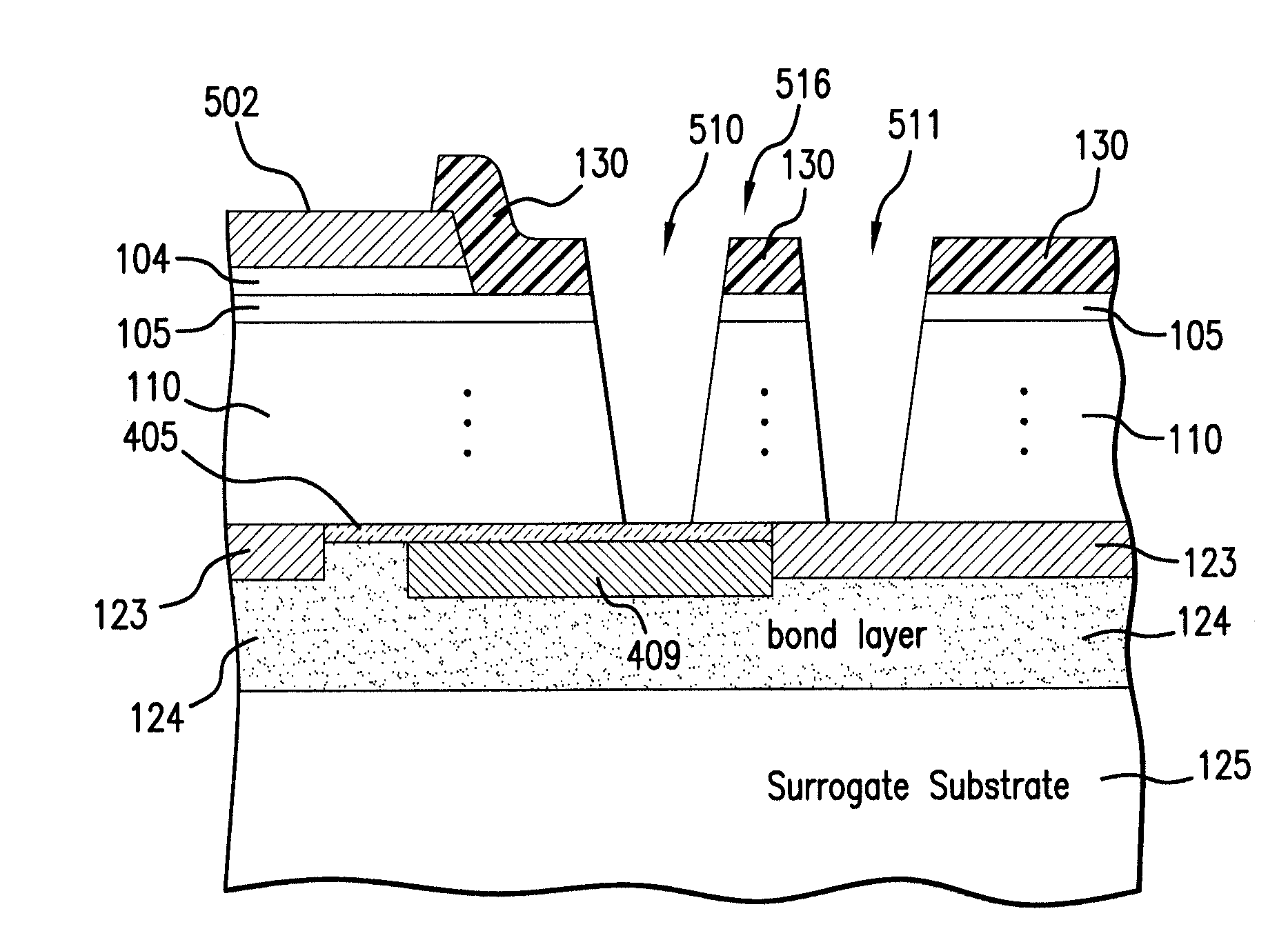
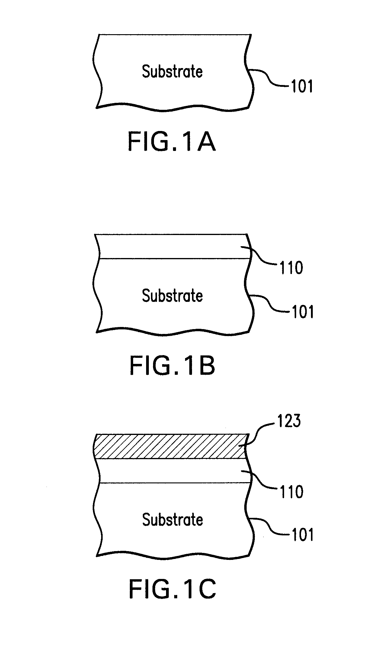
[0053]FIG. 1A is a partial cross-sectional view illustrating a first step of a method for manufacturing a semiconductor-based solar cell, according to an embodiment of the present invention. A first substrate 101 is provided, which can be a semiconductor wafer, for example a GaAs wafer, or any other suitable growth substrate made of a semiconductor material, such as of Ge, InP or GaAs or of other suitable material. With reference to FIG. 1B, a plurality of semiconductor layers are sequentially deposited on substrate 101, which are collectively indicated with referral number 110 and referred to as the semiconductor body. The semiconductor layers comprise for example binary, ternary and / or quaternary alloys of III-V semiconductors (details of the semiconductor layers are not illustrated in the figures). The plurality of semiconductor layers 110 will constitute the absorption portion of the cell, in which the absorption of the sun light takes place.

[0054]In a preferred embodiment, the ...


PUM


Abstract

A method of manufacturing a solar cell by providing a first substrate; depositing sequentially on the first substrate a plurality of semiconductor layers, the plurality of semiconductor layers comprising a first layer and a last layer in the direction of deposition; forming a backside contact layer on the last semiconductor layer; forming on the last semiconductor layer a back cathode contact isolated from at least a first portion of the backside contact layer, the first portion forming the anode contact; attaching a second substrate on the backside contact layer and removing the first substrate to expose the first semiconductor layer and to define a front surface and an opposite back surface of a solar cell; forming a front cathode contact on the front surface of the solar cell; etching a first trench through the plurality of semiconductor layers to define an active portion of the solar cell with a first mesa structure including the front cathode contact and the anode contact and being surrounded by the first trench, the first mesa having a first sidewall in the first trench and a lateral peripheral region beyond the sidewall, and forming in the lateral peripheral region an electrically conductive layer extending from the front surface where it is electrically connected to the front cathode contact along the first sidewall of the first trench to be electrically connected to the back cathode contact.

Description

GOVERNMENT RIGHTS STATEMENT[0001]This invention was made with government support under Contract No. FA9453-06-C-0345 awarded by the U.S. Air Force. The Government has certain rights in the invention.BACKGROUND OF THE INVENTION[0002]1. Field of the Invention[0003]The present invention relates to semiconductor-based solar cells. In particular, the present invention relates to solar cells including integrated semiconductor structures with back-contact cell design and to methods of manufacturing such cells.[0004]2. Description of Related Art[0005]Solar cells are photovoltaic devices that convert sunlight directly into electrical power.[0006]Thin-film technology has gained widespread interest in satellite and in general space applications because of their low cost, high-density packaging, and radiation resistance. Thin-film solar cells can be in general based on different semiconductors materials, such as polycrystalline or amorphous silicon, binary to quaternary alloys of III-V semicond...

Claims


Application Information

Patent Timeline
Patent Type & Authority Applications(United States)
IPC IPC(8): H01L31/00H01L21/28
CPCH01L31/022441Y02E10/544H01L31/1892H01L31/06875Y02P70/50
Inventor CORNFELD, ARTHURDIAZ, JACQUELINE
Owner SOLAERO TECH CORP
Why Eureka
Try Eureka