Adhesive sheet for supporting and protecting semiconductor wafer and method for grinding back of semiconductor wafer

a technology for supporting and protecting semiconductor wafers, applied in the direction of film/foil adhesives, synthetic resin layered products, transportation and packaging, etc., can solve the problems of grinding debris, grinding water, damage to the pattern surface, etc., and achieve the effect of reducing sticky residue and raising product yield

Inactive Publication Date: 2011-02-10
NITTO DENKO CORP
View PDF2 Cites 19 Cited by
  • Summary
  • Abstract
  • Description
  • Claims
  • Application Information

AI Technical Summary

Benefits of technology

[0015]With the adhesive sheet of the present invention, the problem of sticky residue attributable to the irregularities on the pattern formation surface of today's semiconductor wafers can be eff

Problems solved by technology

Damage to the pattern surface, fouling by grinding debris, grinding water, and the like can occur in a back grinding step in which the back of a semiconductor wafer is subjected to polishing and grinding, and in a dicing step in which the wafer is cut into individual chips.
Also, the semiconductor wafer itself is thin and brittle, and in addition there are electrodes and other such protrusions on the pattern surface of the semiconductor wafer, so a problem is that even a slight external force tends to cause damage.
However, as semiconductor devices have become smaller and their density has risen in recent years, the height of the protrusions on the circuit pattern surface of these semiconductor wafers has been on the rise, and the pitch between the protrusions has been decreasing.
Accordingly, with a conventional m

Method used


Image

  • Adhesive sheet for supporting and protecting semiconductor wafer and method for grinding back of semiconductor wafer
  • Adhesive sheet for supporting and protecting semiconductor wafer and method for grinding back of semiconductor wafer

Examples


example 1

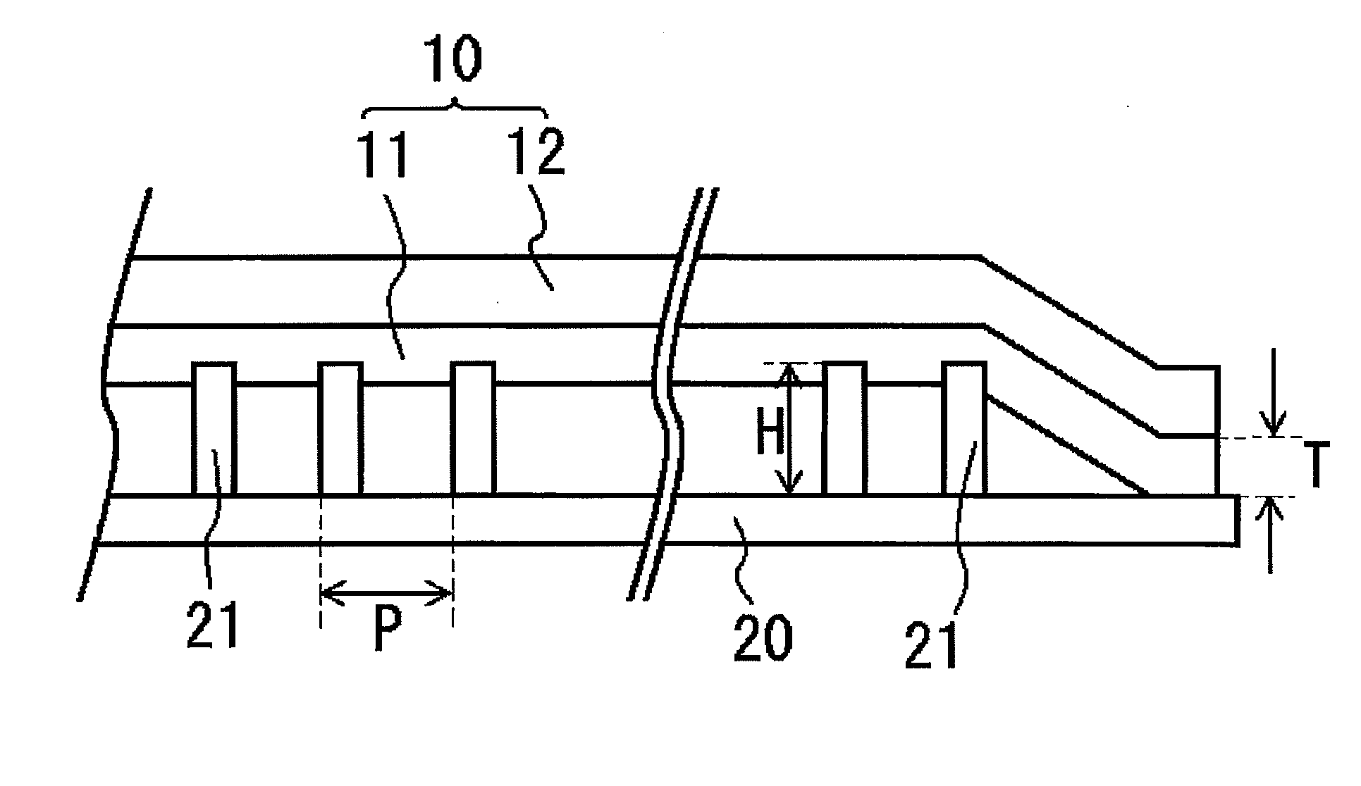
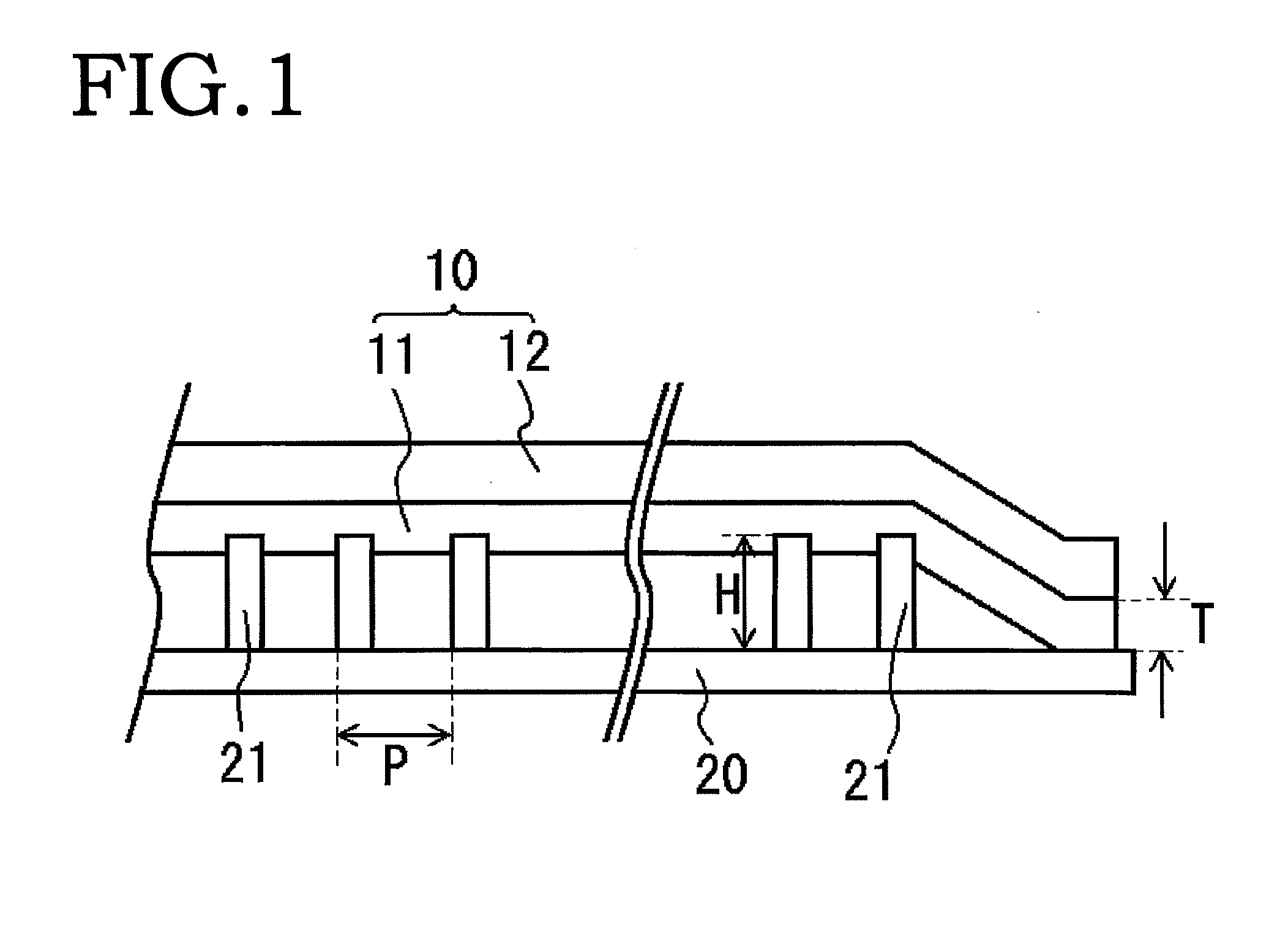
[0138]The 115·m-thick ethylene-vinyl acetate copolymer (EVA) film was used as the base film.

[0139]On the base film, the pressure sensitive adhesive layer (15·m-thick) was formed.

[0140]The resin solution was used to coat a 38·m-thick silicone release-treated polyester film so that the thickness of the resulting film became 50·m after drying and was dried for 2 minutes at 140° C. to form a pressure sensitive adhesive layer of the acrylic adhesive 1.

[0141]Thus obtained pressure sensitive adhesive layer was laminated on the base film to form an adhesive sheet for supporting and protecting a semiconductor wafer and the sheet was aged for 1 day or more at 50° C.

[0142]When the adhesive strength of the sheet to the silicon wafer was measured, the result was 12 N / 20 mm.


PUM

PropertyMeasurementUnit
Temperatureaaaaaaaaaa
Thicknessaaaaaaaaaa
Heightaaaaaaaaaa

Abstract

An adhesive sheet for supporting and protecting a semiconductor wafer has an adhesive layer formed on one side of a base film, the adhesive layer having a thickness of 4 to 42 μm and an elastic modulus at 25° C. of 0.5 to 9 MPa. The adhesive sheet of the present invention is useful in the broader application such as an adhesive sheet for affixing a wafer and for protecting a wafer, and the like in various steps of working the semiconductor wafers, that needs re-peelable.

Description

BACKGROUND[0001]1. Technical Field[0002]The present invention relates to an adhesive sheet for supporting and protecting a semiconductor wafer, and to a method for grinding the back of a semiconductor wafer, and more particularly relates to an adhesive sheet for supporting and protecting a semiconductor wafer and to a method for grinding the back of a semiconductor wafer, which can be used to advantage with semiconductor wafers having protruding bumps on their surface.[0003]2. Related Art[0004]Damage to the pattern surface, fouling by grinding debris, grinding water, and the like can occur in a back grinding step in which the back of a semiconductor wafer is subjected to polishing and grinding, and in a dicing step in which the wafer is cut into individual chips.[0005]Also, the semiconductor wafer itself is thin and brittle, and in addition there are electrodes and other such protrusions on the pattern surface of the semiconductor wafer, so a problem is that even a slight external f...

Claims


Application Information

Patent Timeline
IPC IPC(8): B32B38/10C09J7/02B32B7/02B32B27/30
CPCC09J7/0217C09J2201/622Y10T428/264H01L21/6836H01L2221/6834C09J2203/326C09J7/385C09J2301/312
Inventor SASAKI, TAKATOSHIASAI, FUMITERUMIZUNO, KOUJI
Owner NITTO DENKO CORP
Why Eureka
Try Eureka