Semiconductor device and manufacturing method thereof

a technology of semiconductor devices and semiconductors, applied in semiconductor devices, electrical equipment, instruments, etc., can solve the problems of increased capacity load of thin film transistors, small on-off ratios, and electrical characteristics, and achieve excellent electric characteristics and high reliability

Active Publication Date: 2011-02-10
SEMICON ENERGY LAB CO LTD
View PDF25 Cites 88 Cited by
  • Summary
  • Abstract
  • Description
  • Claims
  • Application Information

AI Technical Summary

Benefits of technology

[0050]A semiconductor device including a thin film transistor which uses an oxide semicondu

Problems solved by technology

However, in the case where the channel length is shortened, a problem of switching characteristics such as a small on-off ratio arises.

Method used


Image

  • Semiconductor device and manufacturing method thereof
  • Semiconductor device and manufacturing method thereof
  • Semiconductor device and manufacturing method thereof

Examples


embodiment 1

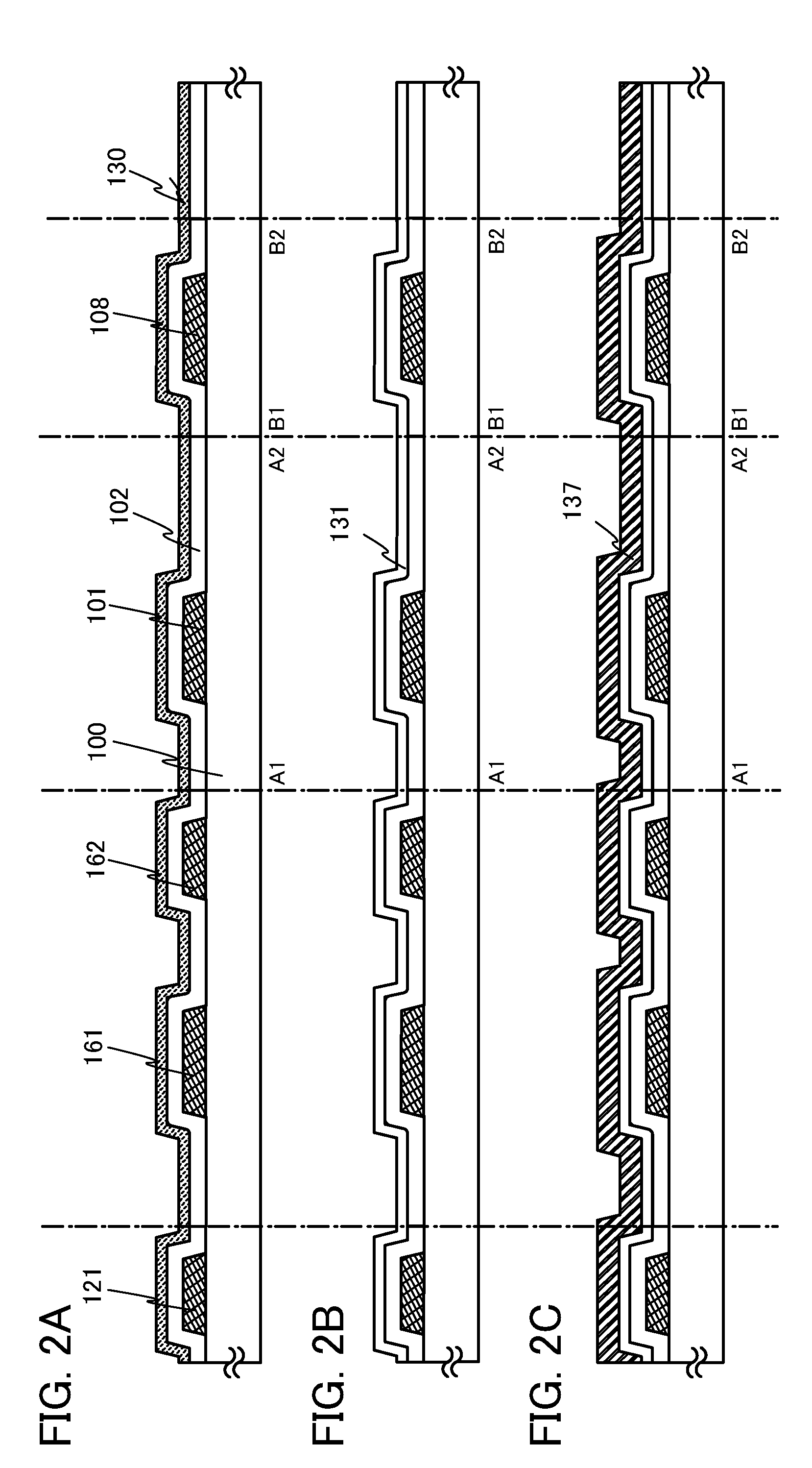
[0087]A manufacturing process of a semiconductor device including a thin film transistor will be described with reference to FIG. 1, FIGS. 2A to 2C, FIGS. 3A and 3B, FIGS. 4A to 4C, and FIG. 5.

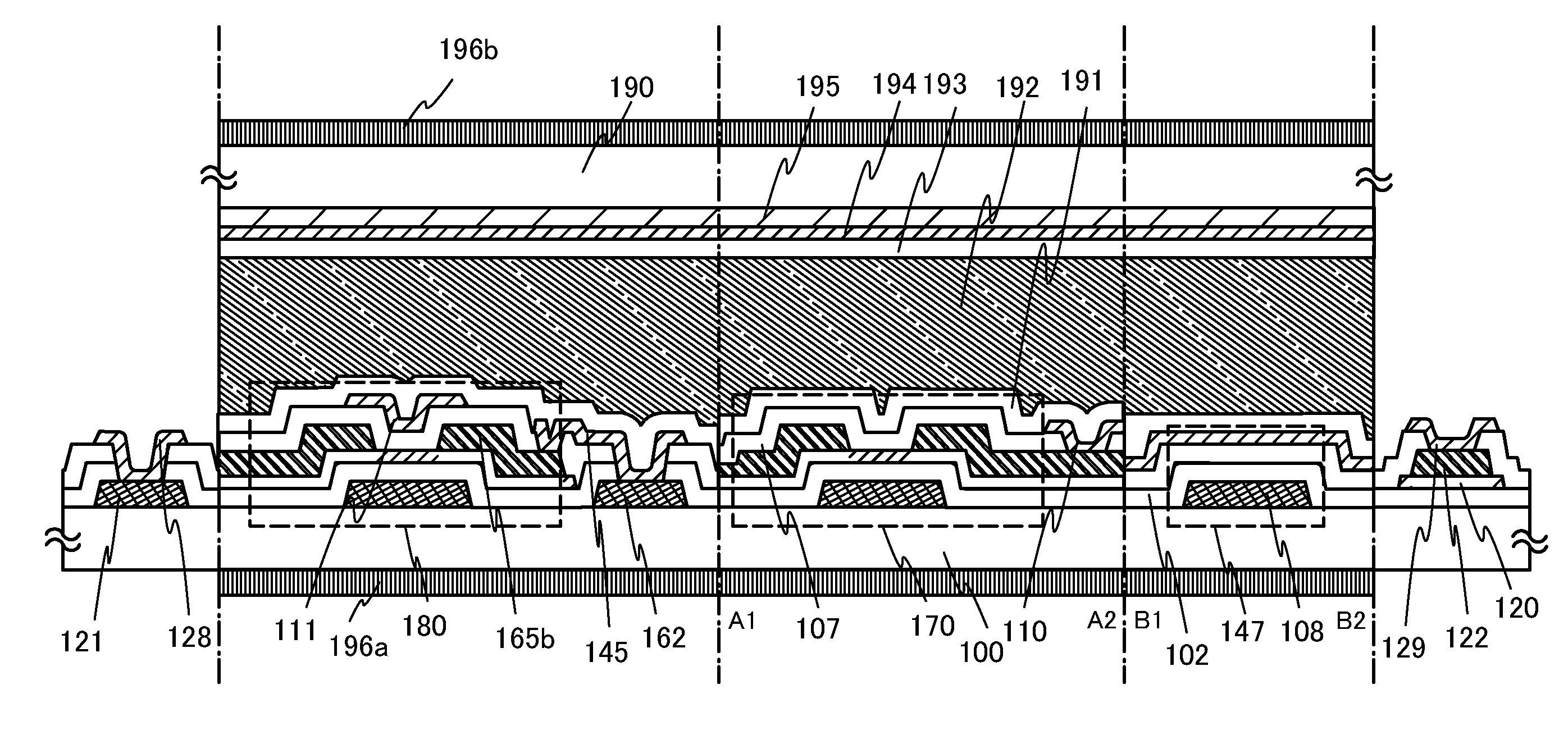
[0088]A liquid crystal display device as a semiconductor device which is one embodiment of the present invention is illustrated in FIG. 1. In the liquid crystal display device in FIG. 1, a substrate 100 which is provided with a pixel portion including a thin film transistor 170 and a capacitor 147, a driver circuit portion including a thin film transistor 180, a pixel electrode layer 110, and an insulating layer 191 serving as an alignment film, and a substrate 190 which is provided with an insulating layer 193 serving as an alignment film, a counter electrode layer 194, and a coloring layer 195 serving as a color filter face each other with a liquid crystal layer 192 positioned between the substrates. The substrate 100 is provided with a polarizing plate (a layer including a polarizer, also s...

embodiment 2

[0186]In this embodiment, an example in which oxide conductive layers serving as source and drain regions are provided between the oxide semiconductor layer and the source and drain electrode layers in Embodiment 1 will be described with reference to FIGS. 6A to 6D and FIGS. 7A and 7B. Therefore, the thin film transistor, except the oxide conductive layers, can be formed in a manner similar to that shown in Embodiment 1; thus, description of the same components or components having the same functions as those in Embodiment, and the manufacturing process thereof will be omitted. FIGS. 6A to 6D and FIGS. 7A and 7B are similar to FIG. 1, FIGS. 2A to 2C, FIGS. 3A and 3B, FIGS. 4A to 4C, and FIG. 5 except that part of the process in FIGS. 6A to 6D and FIGS. 7A and 7B is different from that in FIG. 1, FIGS. 2A to 2C, FIGS. 3A and 3B, FIGS. 4A to 4C, and FIG. 5; thus, the same portions as those in FIG. 1, FIGS. 2A to 2C, FIGS. 3A and 3B, FIGS. 4A to 4C, and FIG. 5 are denoted by the same r...

embodiment 3

[0220]This embodiment shows an example of a liquid crystal display device in which a liquid crystal layer is placed between a first substrate and a second substrate, and a common connection portion is formed over the first substrate so as to be electrically connected to a counter electrode provided on the second substrate. Note that a thin film transistor is formed as a switching element over the first substrate, and the common connection portion is manufactured in the same process as the switching element in a pixel portion, resulting in simplified process.

[0221]The common connection portion is provided in a position overlapping with a sealant for attaching the first substrate and the second substrate to each other and is electrically connected to a counter electrode through conductive particles in the sealant. Alternatively, the common connection portion is provided in a position which does not overlap with the sealant (except for the pixel portion) and a paste including conductiv...


PUM


Abstract

An object is to improve reliability of a semiconductor device. A semiconductor device including a driver circuit portion and a display portion (also referred to as a pixel portion) over the same substrate is provided. The driver circuit portion and the display portion include thin film transistors in which a semiconductor layer includes an oxide semiconductor; a first wiring; and a second wiring. The thin film transistors each include a source electrode layer and a drain electrode layer which each have a shape whose end portions are located on an inner side than end portions of the semiconductor layer. In the thin film transistor in the driver circuit portion, the semiconductor layer is provided between a gate electrode layer and a conductive layer. The first wiring and the second wiring are electrically connected in an opening provided in a gate insulating layer through an oxide conductive layer.

Description

BACKGROUND OF THE INVENTION[0001]1. Field of the Invention[0002]The present invention relates to a semiconductor device including an oxide semiconductor.[0003]In this specification, a semiconductor device means all types of devices which can function by utilizing semiconductor characteristics, and an electro-optical device such as a liquid crystal display device, a semiconductor circuit, and an electronic device are all semiconductor devices.[0004]2. Description of the Related Art[0005]In recent years, a technique for forming a thin film transistor (TFT) by using a semiconductor thin film (having a thickness of approximately several nanometers to several hundreds of nanometers) formed over a substrate having an insulating surface has attracted attention. Thin film transistors are applied to a wide range of electronic devices such as integrated circuits (ICs) and electro-optical devices, and thin film transistors that are used as switching elements in image display devices are, in pa...

Claims


Application Information

Patent Timeline
IPC IPC(8): H01L33/40H01L33/38H01L33/36
CPCH01L27/1214H01L27/1225H01L33/0041H01L27/1288H01L2924/0002H01L27/1251H01L2924/00H01L27/124H01L27/1255H01L27/127G02F1/136227G02F1/1368H01L29/45H01L21/385H01L29/4908H01L29/78648H01L29/7869
Inventor YAMAZAKI, SHUNPEISAKATA, JUNICHIROSAKAKURA, MASAYUKIOIKAWA, YOSHIAKIOKAZAKI, KENICHIMARUYAMA, HOTAKA
Owner SEMICON ENERGY LAB CO LTD
Why Eureka
Try Eureka