

Thin film transistor
- Summary
- Abstract
- Description
- Claims
- Application Information
AI Technical Summary
Benefits of technology
Problems solved by technology
Method used
Image

Examples
Embodiment Construction
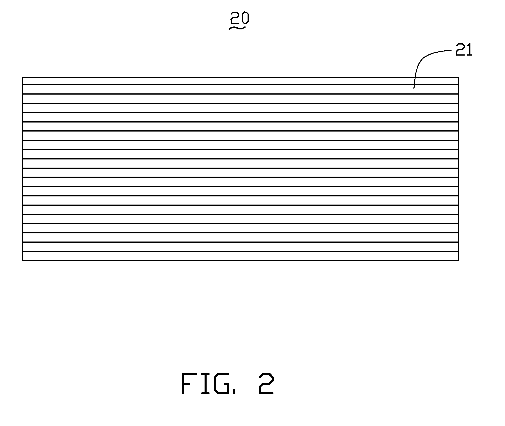
[0014]The disclosure is illustrated by way of example and not by way of limitation in the figures of the accompanying drawings in which like references indicate similar elements. It should be noted that references to “an” or “one” embodiment in this disclosure are not necessarily to the same embodiment, and such references mean at least one.
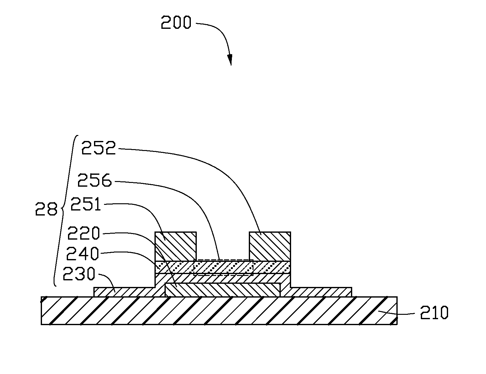
[0015]Referring to FIG. 1, a thin film transistor 10 of one embodiment is applied in a thin film transistor panel 100. The thin film transistor panel 100 can include an insulating substrate 110 and a plurality of thin film transistors 10 (only one is shown in the FIG. 1) located thereon.
[0016]The insulating substrate 110 is provided for supporting the thin film transistors 10. The material of the insulating substrate 110 can be the same as a substrate of a printed circuit board (PCB), and can be rigid materials (e.g., p-type or n-type silicon, silicon with an silicon dioxide layer formed thereon, crystal, crystal with a oxide layer formed thereon...
PUM
 Abstract
Description
Claims
Application Information