Wafer probe test and inspection system

a wafer probe and inspection system technology, applied in the field of electric test methods and equipment, can solve the problems of higher probe force, poor return on investment of the probe, and related compromise between hardware accuracy and weight in the probe, so as to reduce hardware costs, increase the utilization rate of the tester, and reduce the cost of the conventional probe

Inactive Publication Date: 2011-02-17
RUDOLPH TECHNOLOGIES INC
View PDF4 Cites 21 Cited by
  • Summary
  • Abstract
  • Description
  • Claims
  • Application Information

AI Technical Summary

Benefits of technology

[0012]In certain embodiments, a system for wafer prealignment onto carrier plates, or wafer carriers, is provided. Once the wafer is prealigned onto a wafer carrier, further automated wafer alignment is unnecessary. The wafer carrier itself may incorporate universal mounting and alignment hardware that facilitates alignment with test equipment. The hardware at the test location also becomes more simplified. The test equipment simply incorporates mounting hardware that is complementary to, or otherwise operable to receive the wafer carrier mounting hardware. X-Y wafer indexing required for some current multiple touchdown wafer testing may be enabled through placing the wafer carrier into multiple tooling locations at the test equipment. The wafer alignment hardware may further employ wafer inspection functionality and thereby provide for pre- and post-probe inspection of the wafer. Various software modules may utilize the acquired wafer inspection data in order to provide detailed pre-probe wafer analysis, as well as post-probe wafer analysis operable to evaluate the entire wafer test process and, ultimately, process yield management.
[0013]Certain aspects of the present invention provide various benefits over conventional wafer testing methods. First, the present invention reduces hardware costs because the conventional prober is eliminated. Second, the present invention increases tester utilization because wafer lots can be broken down and shared between multiple test equipment rather than waiting in a single prober. Third, better process control is provided because wafer alignment does not depend upon individual prober performance at each test location. Fourth, according to certain aspects of the present invention a “lights-out” wafer test floor is possible. Fifth, features of the present invention anticipate the demands of future semiconductor testing, including the need to probe even smaller and more densely positioned bonding pads, by providing probing solutions that minimize fixture deflection and employ more constant probe force. Finally, aspects of the present invention provide for higher reliability through the simplification of the entire wafer test process and great error budget control.

Problems solved by technology

First, the long test times mean that the prober 22 indexing and alignment hardware is underutilized resulting in a poor return on investment for the probers 22 and in some instances, testers 20 as well.
These changes have, in turn, resulted in higher probe forces and a related compromise between hardware accuracy and weight in probers 22.
This results in the non-optimal use of floor space.
Fourth, as tester complexity increases, there is a high volume of interconnects between components and a greater potential for reliability problems.

Method used


Image

  • Wafer probe test and inspection system
  • Wafer probe test and inspection system
  • Wafer probe test and inspection system

Examples


Embodiment Construction

[0026]In the following detailed description of the invention, reference is made to the accompanying drawings that form a part hereof, and in which is shown, by way of illustration, specific embodiments in which the invention may be practiced. In the drawings, like numerals describe substantially similar components throughout the several views. These embodiments are described in sufficient detail to enable those skilled in the art to practice the invention. Other embodiments may be utilized and structural, logical, and electrical changes may be made without departing from the scope of the present invention. The following detailed description is, therefore, not to be taken in a limiting sense, and the scope of the present invention is defined only by the appended claims and equivalents thereof.

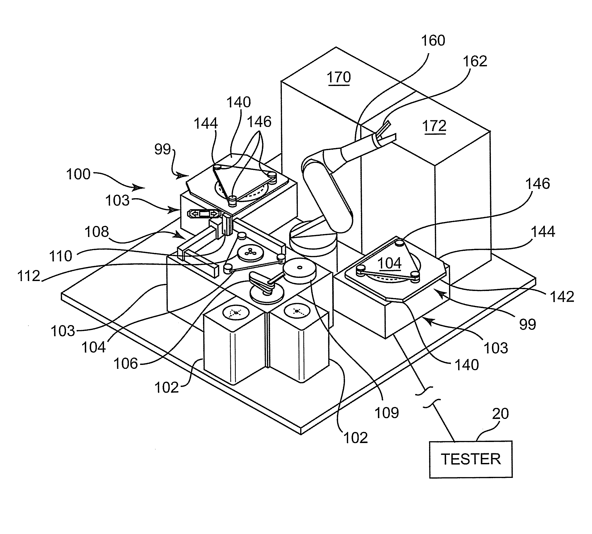
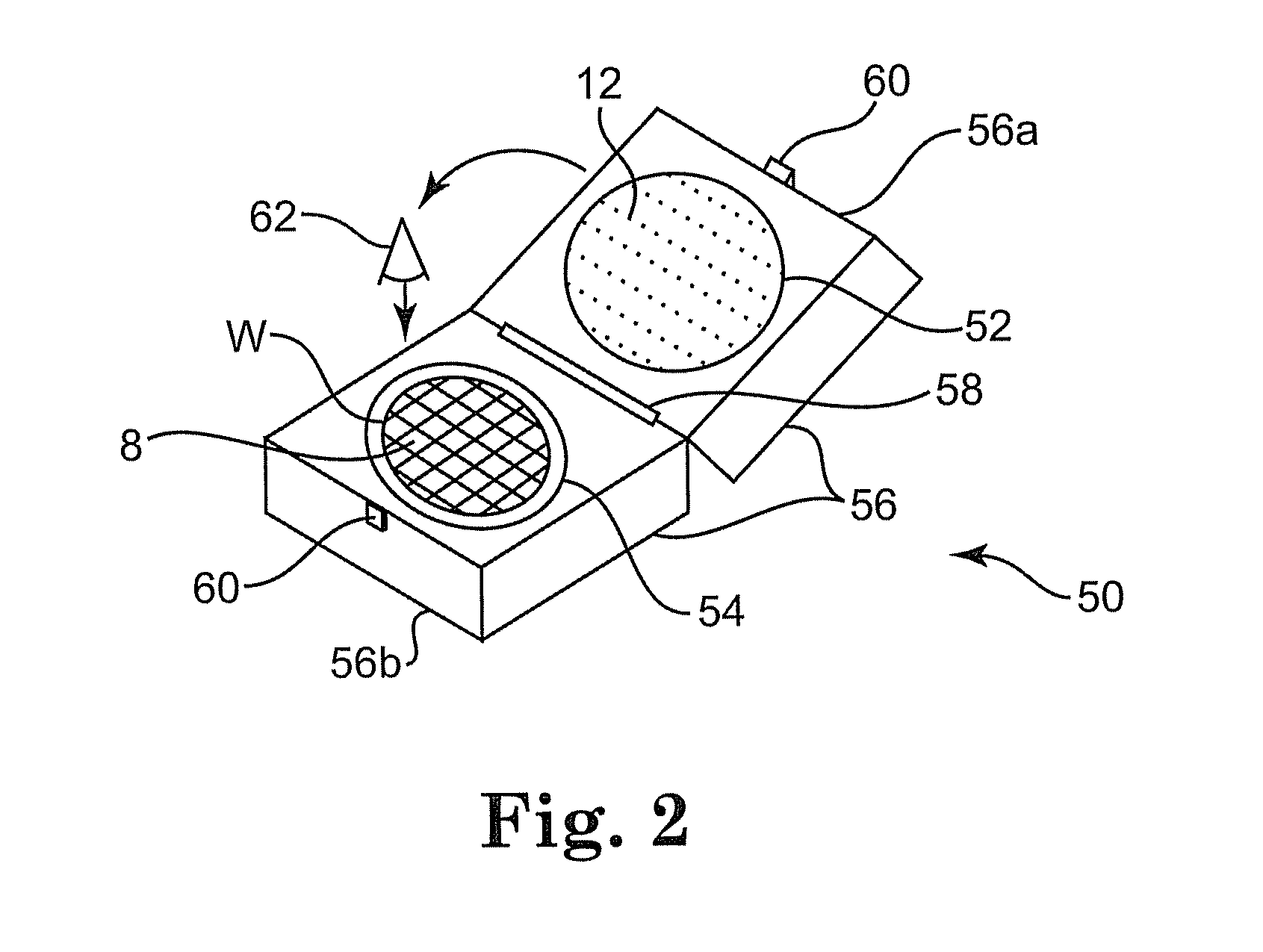
[0027]FIG. 2 illustrates an embodiment of the present invention useful for increasing utilization of a test cell. Cassette 50 includes a probe card 52 and a wafer stage 54 mounted within a housi...


PUM


Abstract

An apparatus for electrically testing a semiconductor device is herein disclosed. The apparatus includes carriers for a semiconductor device and a probe card (52) that are adapted for complementary registration with one another. The coupled carriers may be stacked or used in another high-density arrangement during electrical test or burn-in to improve test cell utilization.

Description

CROSS-REFERENCE TO RELATED APPLICATIONS[0001]This is application is related to International Patent Application No. PCT / US2008 / 063779, filed on 15 May 2008, which claims priority from U.S. Provisional Patent Application No. 60 / 938,142, filed on 15 May 2007.TECHNICAL FIELD OF THE INVENTION[0002]The present invention relates to the field of electrical test methods and equipment. More particularly, this invention relates to methods and systems for the high-parallelism testing and pre and post-probe inspection and analysis of semiconductor wafers.BACKGROUND OF THE INVENTION[0003]In the semiconductor industry, many replicate components, or die, are created on a single silicon wafer. In order to eliminate faulty die prior to the cost intensive step of packaging, semiconductor fabricators typically perform wafer testing or sorting. One facet of wafer testing typically consists of establishing electrical connectivity between the metalized bond pads or bumps contained on each individual die ...

Claims


Application Information

Patent Timeline
Patent Type & Authority Applications(United States)
IPC IPC(8): G01R31/00G01R31/26
CPCG01R1/0491H01L21/68H01L22/00
Inventor SEUBERT, RONALD C.HILTON, GEOFFREYSANDBACH, REX H.
Owner RUDOLPH TECHNOLOGIES INC
Why Eureka
Try Eureka