Solid-state imaging device, data transfer circuit, and camera system

Inactive Publication Date: 2011-02-17
SONY CORP
View PDF8 Cites 19 Cited by
  • Summary
  • Abstract
  • Description
  • Claims
  • Application Information

AI Technical Summary

Benefits of technology

According to the present invention, as the capturing timing of the capturing unit is set as the timing at which both the dummy data output from the far end and the dummy data output from the near end can be captured, the operation margin of the solid-state image pickup element is improved.

Problems solved by technology

However, it takes considerable labor hours to perform these, and it is conceivable that the execution is difficult.

Method used


Image

  • Solid-state imaging device, data transfer circuit, and camera system
  • Solid-state imaging device, data transfer circuit, and camera system
  • Solid-state imaging device, data transfer circuit, and camera system

Examples


first embodiment

[Apparatus Overall Configuration Example]

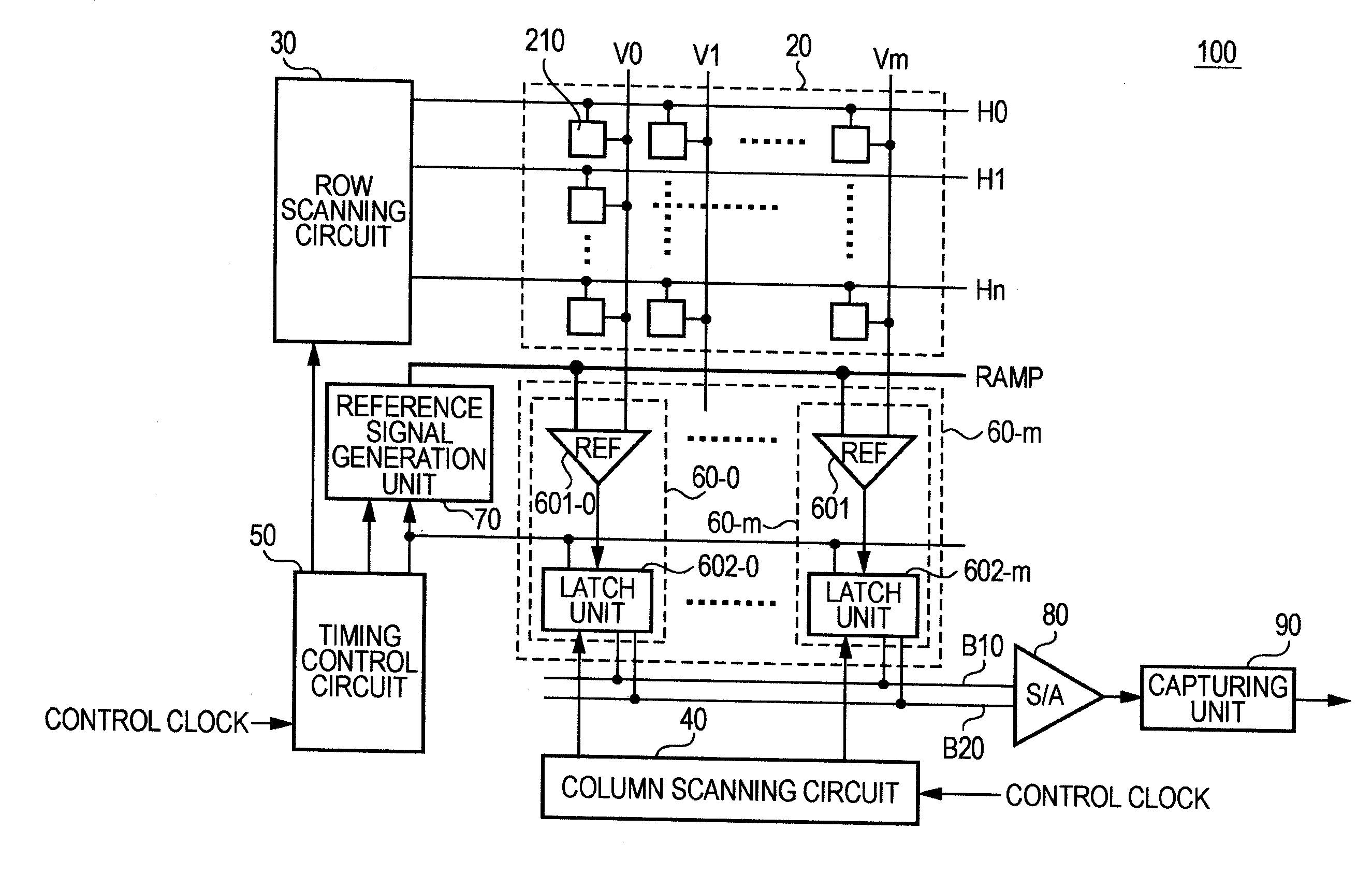
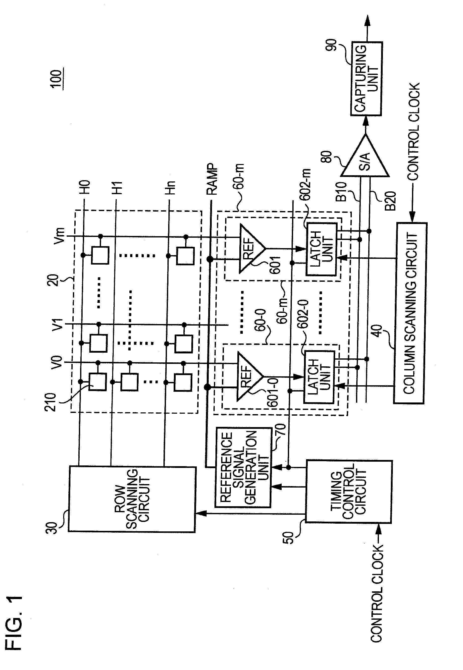
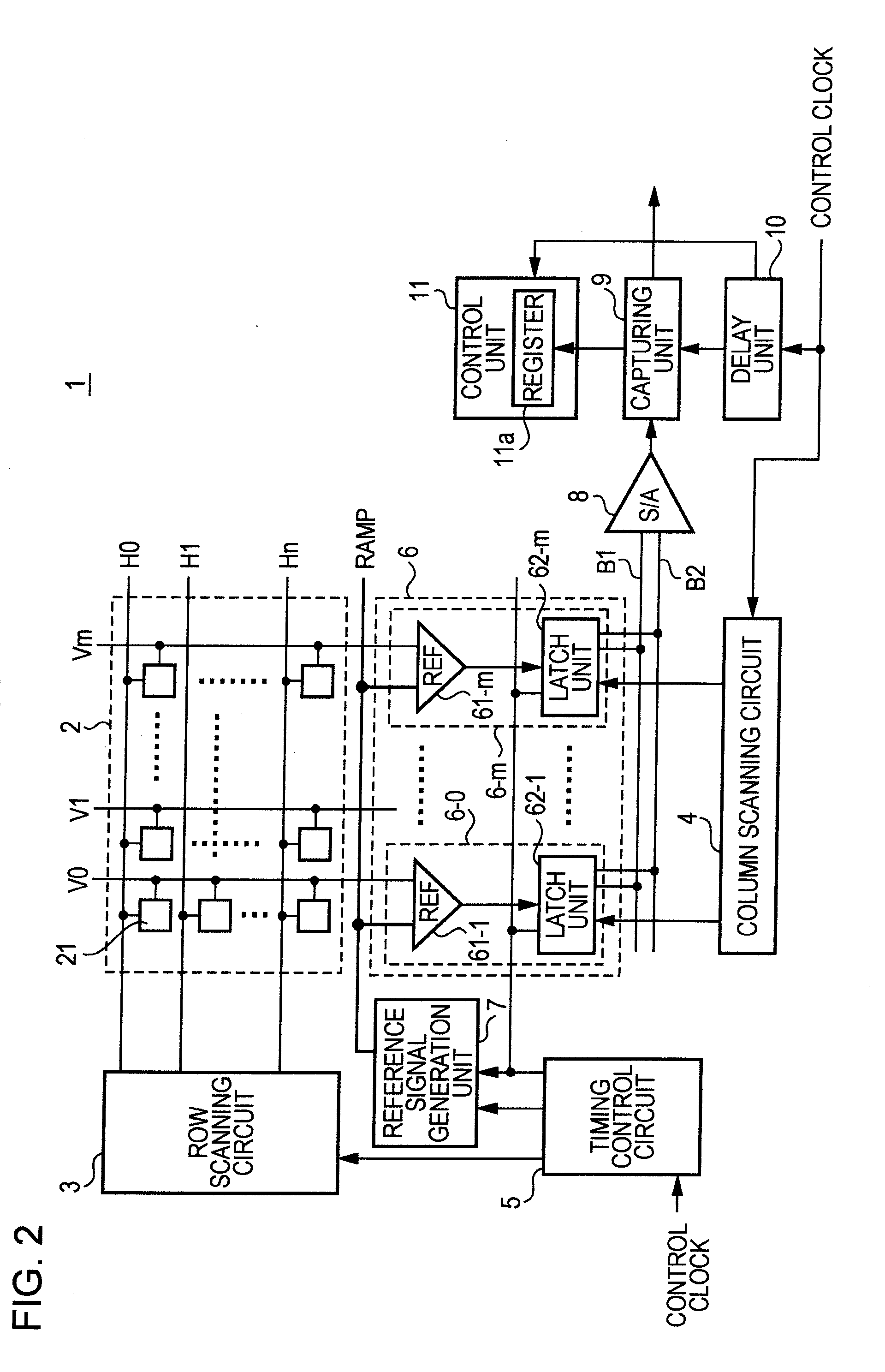
FIG. 2 is a block diagram showing a configuration example of a solid-state image pickup element according to a first embodiment. A solid-state image pickup element 1 shown in FIG. 2 has a pixel array unit 2 composed by arranging pixels 21 in m columns lengthwise and n rows crosswise in a matrix manner, a row scanning circuit 3, a column scanning circuit 4, and a timing control circuit 5.

Also, the solid-state image pickup element 1 is provided with an ADC 6-0 to an ADC 6-m provided while corresponding to the respective columns of the pixel array unit 2 and a reference signal generation unit 7 for supplying a reference voltage RAMP for the A / D conversion to the ADC 6-0 to the ADC 6-m. The ADC 6-0 to the ADC 6-m are respectively provided with a comparator (REF) 61-0 to a comparator 61-m and a latch unit 62-0 to a latch unit 62-m.

The solid-state image pickup element 1 further has a sense amplifier 8, the capturing unit 9, a delay unit 10, and a ...

second embodiment

Next, a second embodiment of the present invention will be described with reference to FIG. 7 and FIG. 8. According to the present embodiment, by using two pairs of bus lines, the output of the dummy data from the far end and the output of the dummy data from the near end are performed at the same time, and a timing at which both the dummy data can be captured is searched for. Then, the timing at which both the dummy data output from both the far end and the near end can be captured is newly set as the capturing timing in the capturing unit 9.

FIG. 7 is a block diagram showing a configuration example of a solid-state image pickup element 1′ according to the present example. In FIG. 7, parts corresponding to FIG. 2 are assigned with the same reference symbols. Also, in FIG. 7, the illustrations of the pixel array unit 2, the row scanning circuit 3, the timing control circuit 5, and the comparator 61 are omitted.

FIG. 7 illustrates an i-th latch unit 62-0i to latch unit 62-mi and an i+1...


PUM


Abstract

To make it possible to appropriately set a capturing timing for a pixel value.For this, the present invention includes a pixel array unit 2 composed of pixels 21 arranged in a row direction and a column direction in a matrix manner and a latch unit 62 provided for each column constituting the pixel array unit 2 and configured to convert a pixel value of the pixel 21 into a digital pixel value to hold the pixel value. Also, the present invention includes a column scanning unit 4 for selecting the latch unit 62, a capturing unit 9 for sequentially capturing the pixel value held by the latch unit selected by the column scanning unit 4 in synchronism with a predetermined clock, and a delay unit 10 for delaying a clock for driving the capturing unit 9 in a plurality of stages. With the configuration described above, first dummy data is set in the latch unit 62-m at the near end, and second dummy data is set in the latch unit 62-0 at the far end. Then, a delay amount in the delay unit 10 is set as a delay amount at which both the first dummy data and the second dummy data can be captured by the capturing unit 9.

Description

TECHNICAL FIELDThe present invention relates to a solid-state image pickup element and a data transfer circuit for transferring a pixel value obtained by the solid-state image pickup element, as well as a camera system into which the solid-state image pickup element is incorporated, and particularly relates to a technology of adjusting a capturing timing for the pixel value in the solid-state image pickup element.BACKGROUND ARTUp to now, as a solid-state image pickup element, a CMOS (Complementary Metal Oxide Semiconductor) type image sensor is known. As the CMOS image sensor is fabricated on a base of a CMOS LSI manufacturing process, it is possible to easily incorporate a function other the image sensor in the same chip through an application of this process. By utilizing this characteristic, an analog digital converter (which will be hereinafter referred to as ADC) is provided for each column of pixels, and a conduct of a conversion processing into a digital signal is performed i...

Claims


Application Information

Patent Timeline
IPC IPC(8): H04N5/228H04N5/335H04N5/341H04N5/374H04N5/378
CPCH04N5/378H04N25/78H04N25/75
Inventor SUZUKI, MISAO
Owner SONY CORP
Why Eureka
Try Eureka