Semiconductor device and manufacturing method thereof
a technology of semiconductors and semiconductors, applied in the direction of semiconductor devices, electrical devices, transistors, etc., can solve the problems of difficult to suppress junction leakage, difficult to control impurity diffusion, and increase the imbalance between nmos and pmos, so as to improve carrier mobility, suppress junction leakage, and increase carrier speed
- Summary
- Abstract
- Description
- Claims
- Application Information
AI Technical Summary
Benefits of technology
Problems solved by technology
Method used
Image

Examples
first embodiment
[Layout of a Semiconductor Device]
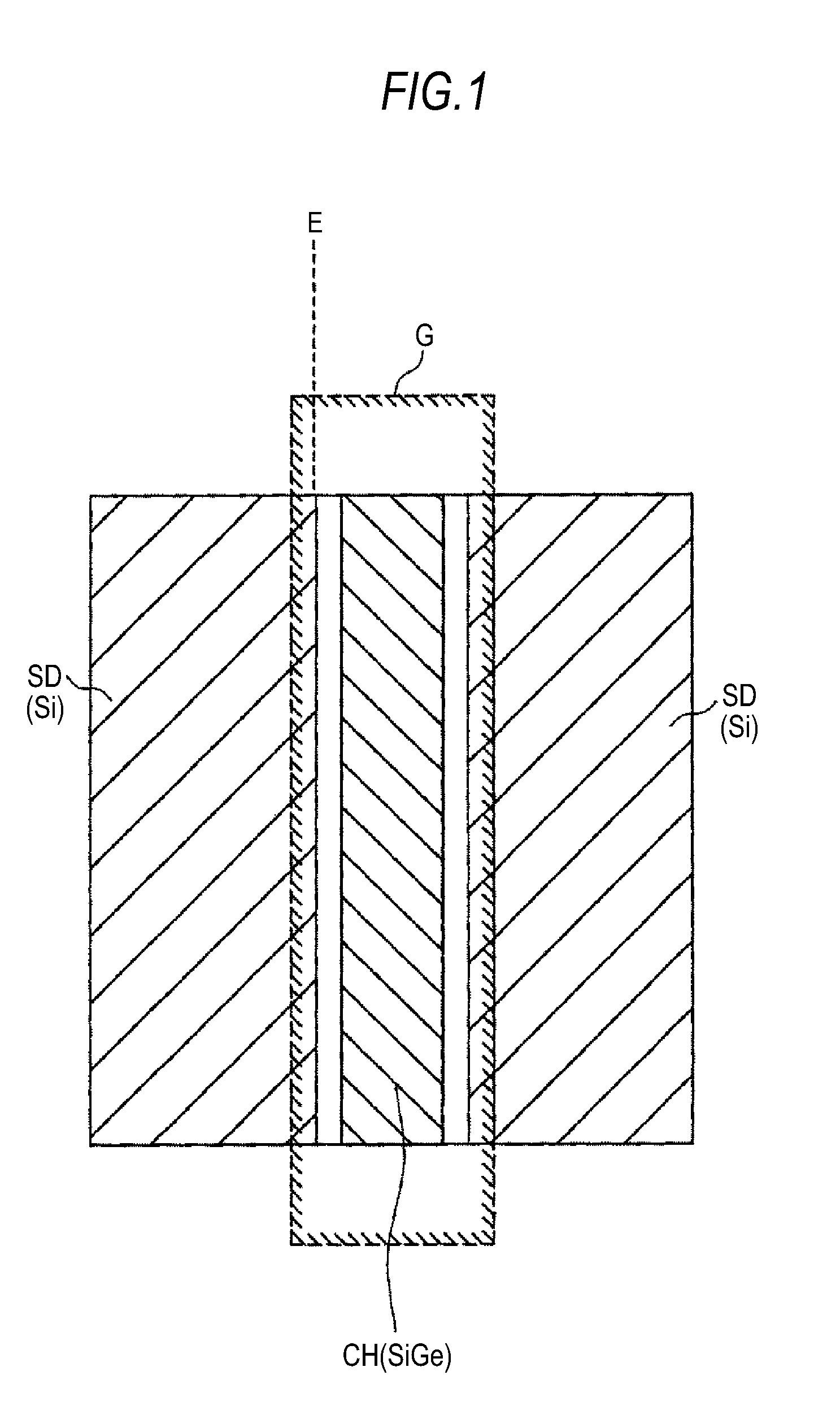
[0072]FIG. 1 is a schematic plan view of a semiconductor device according to the embodiment. The semiconductor device according to the embodiment is a P-channel type MOS field effect transistor (referred to as a PMOS in the following description).
[0073]In a semiconductor substrate made of n-type silicon (Si) or an n-well of the semiconductor substrate, an n-type SiGe layer having a first width in a channel direction is embedded in a channel forming region CH.
[0074]A gate insulating film is formed on the channel forming region and a gate electrode G having a region protruding from the forming region of the SiGe layer is formed with a second width wider than the first width.
[0075]P-type source / drain regions SD having p-type extension regions are formed on the semiconductor substrate sandwiching the channel forming region CH. In the drawing, the source / drain regions having extension regions are not discriminated.
[0076]In the manner as described above, ...
second embodiment
[Cross-Sectional Structure of a Semiconductor Device]
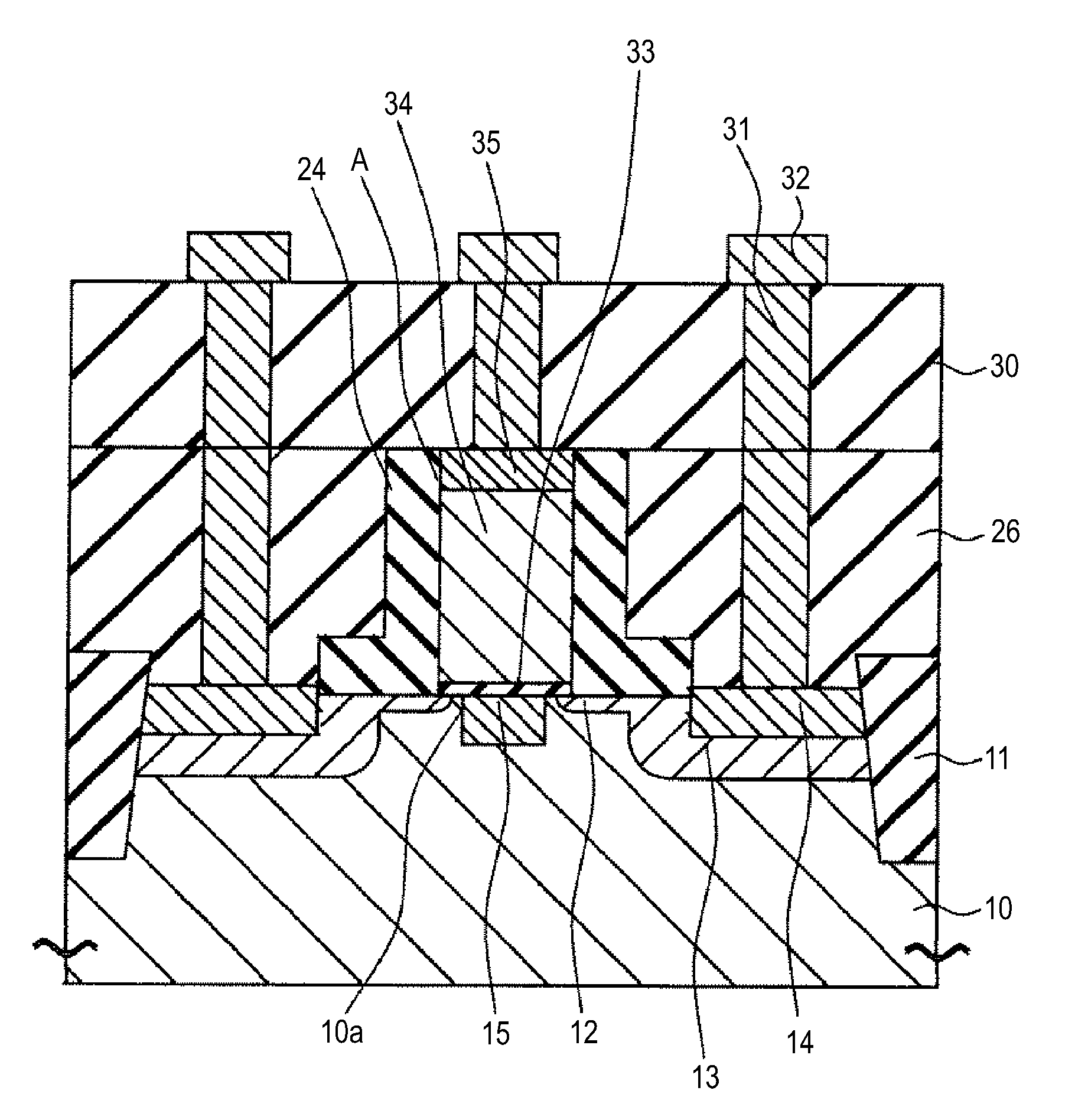
[0139]FIG. 13 is a cross-sectional view of a semiconductor device according to the embodiment.
[0140]For example, a gate insulating film 33 made of silicon oxide and so on is formed on a bottom of the groove for the gate electrode “A”. A gate electrode 34 made of polysilicon is formed in the groove for the gate electrode “A” in the upper layer of the gate insulating film 33. A refractory metal silicide layer 35 made of NiSi and the like is formed at an upper surface of the gate electrode 34.
[0141]The device has the same structure as the first embodiment except the above.
[0142]In the transistor according to the embodiment, the gate electrode is formed with the second width wider than the first width of the SiGe layer at the region protruding from the forming region of the SiGe layer. Additionally, the transistor is formed so that the depletion layer extending from the junction surface between the extension region included in the sou...
third embodiment
[Cross-Sectional Structure of a Semiconductor Device]
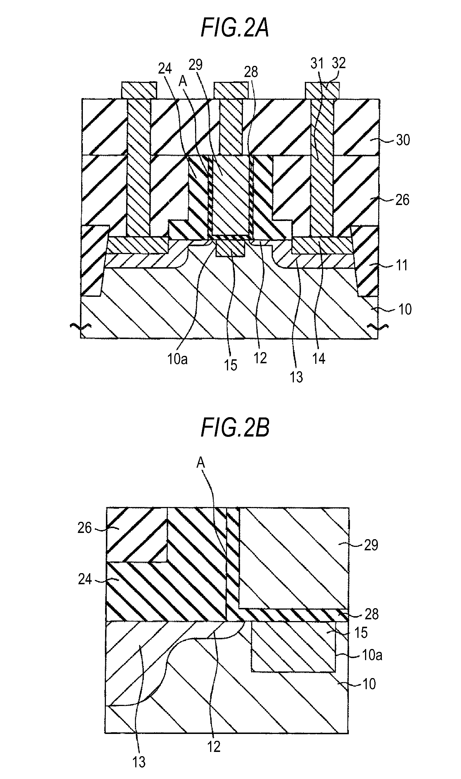
[0156]FIG. 17A is a cross-sectional view of a semiconductor device according to the embodiment, and FIG. 17B is an enlarged view of a part in the vicinity of the extension region, the gate electrode and the SiGe layer, which is the part of FIG. 17A.
[0157]For example, a concave portion for embedding the SiGe layer 10b has a region in which the width in the channel direction becomes wider as the depth from the surface of the semiconductor device 10 becomes deeper. Therefore, the SiGe layer 15 embedded in the concave portion for embedding the SiGe layer 10b has the region in which the width in the channel direction becomes wider as the depth from the surface of the semiconductor device 10 becomes deeper.
[0158]The device has the same structure as the first embodiment except the above.
[0159]In the transistor according to the embodiment, the gate electrode is formed with the second width wider than the first width of the SiGe layer at t...
PUM
 Abstract
Description
Claims
Application Information
 - R&D
- Intellectual Property
- Life Sciences
- Materials
- Tech Scout
- Unparalleled Data Quality
- Higher Quality Content
- 60% Fewer Hallucinations
Browse by: Latest US Patents, China's latest patents, Technical Efficacy Thesaurus, Application Domain, Technology Topic, Popular Technical Reports.
© 2025 PatSnap. All rights reserved.Legal|Privacy policy|Modern Slavery Act Transparency Statement|Sitemap|About US| Contact US: help@patsnap.com