

Compact On-Chip Branchline Coupler Using Slow Wave Transmission Line
a transmission line and branchline coupler technology, applied in waveguides, semiconductor devices, diodes, etc., can solve the problems of large parasitic capacitance, high losses in on-chip passive components, and conventional couplers tend to consume expensive chip area, and achieve large capacitance per unit length , the effect of large inductan
- Summary
- Abstract
- Description
- Claims
- Application Information
AI Technical Summary
Benefits of technology
Problems solved by technology
Method used
Image

Examples
Embodiment Construction
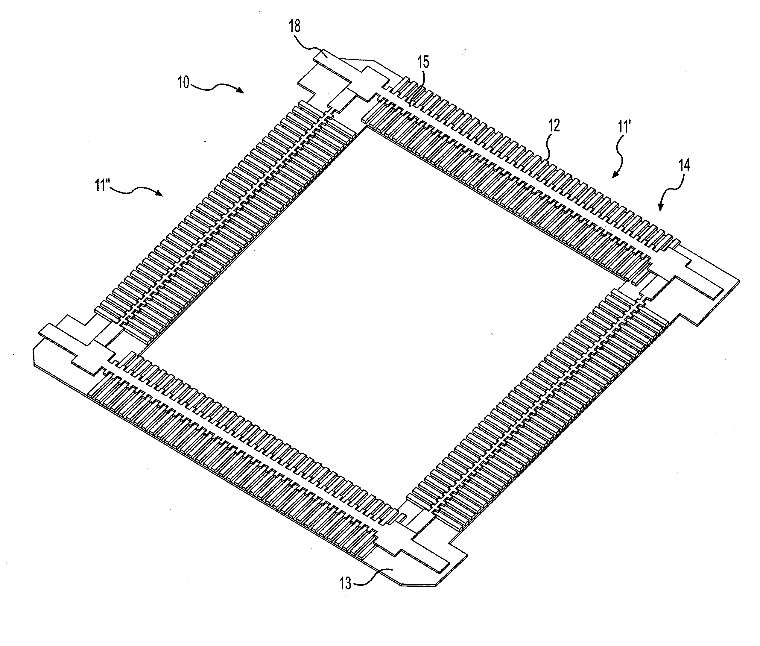
The invention relates to an on-chip branchline coupler, and in particular to an on-chip branchline coupler on slow wave structures with CMOS fabrication technology using multi-layer.
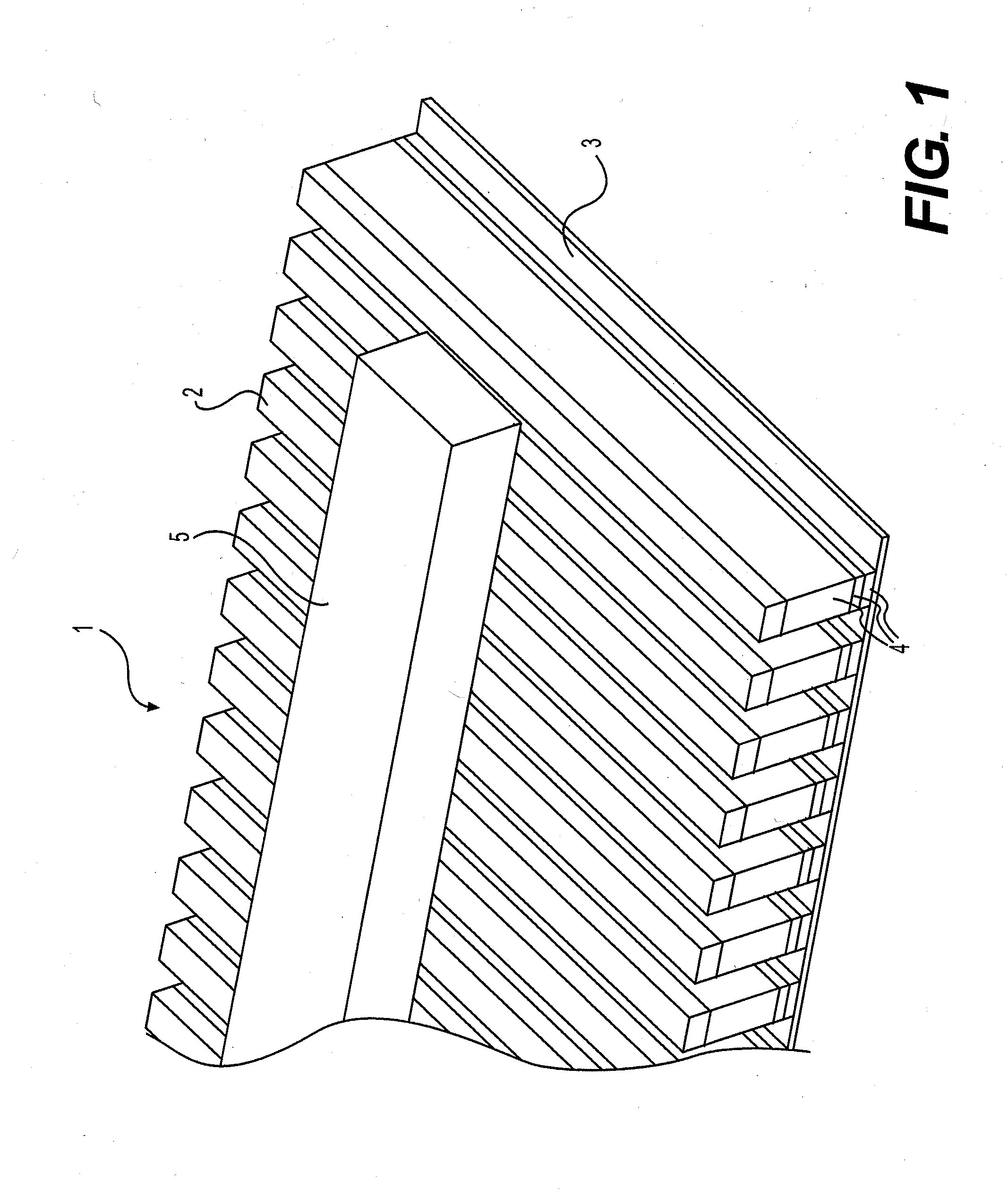
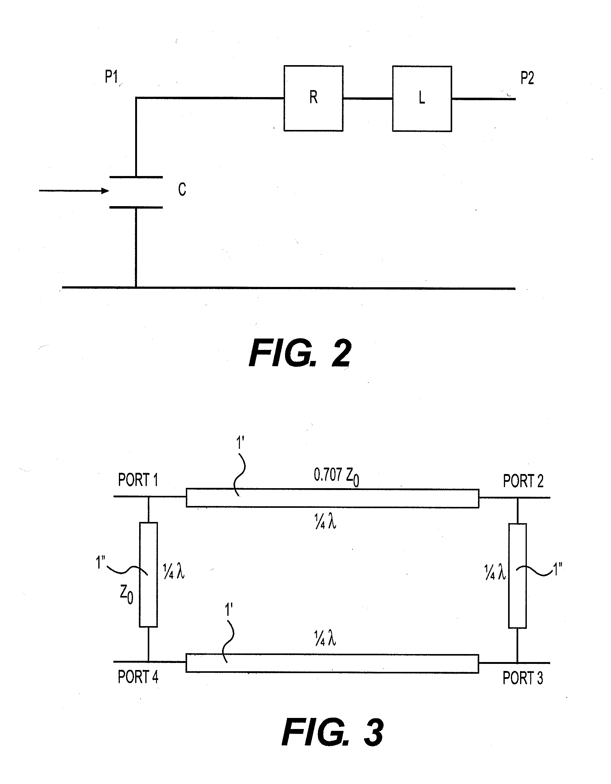
Embodiments of the invention are directed to an on-chip branchline coupler on slow wave structures with CMOS fabrication technology using multi-layer structures. In particular, a current transmission line model can be used for the design of such a slow wave structure.
According to embodiments of the invention, a novel on-chip compact branchline coupler has a slow wave structure and a special multi-layer structure. The structure includes a discontinuous transmission line with metal strips crossing below the signal line. Further, embodiments of the coupler have a more compact size when compared with current traditional structure, e.g., the area can be reduced up to 50%.
Further embodiments of the invention are directed to an ideal on-chip compact branchline coupler using current process technologies, e.g., I...
PUM
 Abstract
Description
Claims
Application Information