
Structural vibration damping device
a technology of structural vibration and damping device, which is applied in the direction of vibration suppression adjustment, mechanical equipment, generator/motor, etc., can solve the problems of excessive weight of the required coil, large inductance, and essential need for supply of control-circuit driving power, so as to reduce installation costs, improve reliability and maintainability, and high performance
- Summary
- Abstract
- Description
- Claims
- Application Information
AI Technical Summary
Benefits of technology
Problems solved by technology
Method used
Image

Examples
first embodiment
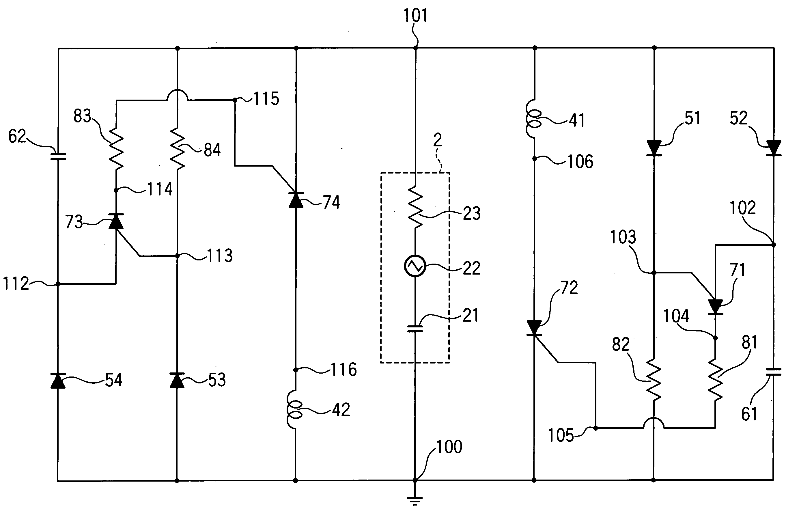
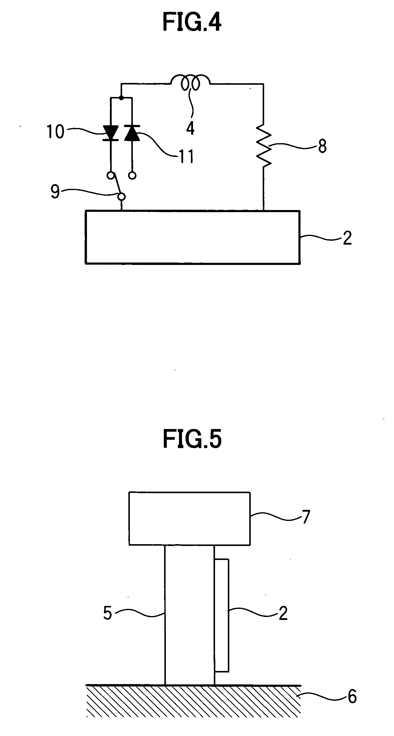
[0050] Referring to FIG. 5, a dead-weight 7 is supported relative to a stationary base 6 through a structure 5. A piezoelectric element 2 is mounted on the structure 5. In conjunction with a displacement of the dead-weight 7, a strain occurs in the piezoelectric element, and a voltage is generated between two electrodes of the piezoelectric element. A circuit illustrated in FIG. 6 is joined to the piezoelectric element 2. In FIG. 6, the piezoelectric element 2 is illustrated as a combination of a capacitor 21, a voltage generator 22 and a resistor 23.
[0051] In this arrangement, a discussion will be firstly made in an initial state when no electric charge is accumulated in the capacitor 21, and the dead-weight 7 is vibrated and moved in a positive direction. As described above, a voltage is generated between the electrodes of the piezoelectric element in conjunction with the movement of the dead-weight 7 in the positive direction. This is equivalent to a state when a positive voltag...
second embodiment
[0063] As shown in FIG. 8, a plurality of dead-weights each having a weight of 0.5 kg are mounted on a trussed structure having an overall length of 3.8 m and a total mass of about 7.9 kg, and a commercially available piezoelectric element “ASB171C801NPO” (produced by NEC TOKIN Co.) is incorporated in a member 13 of the trussed structure. This trussed structure has a primary natural frequency of about 11.3 Hz. A shunt circuit as shown in FIG. 7 is connected between two electrodes of the above piezoelectric element. Based on the circuit illustrated in FIG. 6, the circuit illustrated in FIG. 7 additionally includes two resisters 85, 86 to prevent the circuit from too sensitively responding to an unwanted voltage variation mixed in a voltage generated by the piezoelectric element due to a higher mode vibration.
[0064] In FIG. 7, each of the coils 41, 42 has an inductance of 10 mH, and each of the capacitors 61, 62 has a capacitance of 0.1 μF. Each of the resistors 81, 83 has a resistan...
third embodiment
[0067] In the first and second embodiments, two different coils are used for each of the currents flowing across the shunt circuit in the positive direction and in the negative direction. FIG. 10 shows a shunt circuit using a single common coil for both the currents flowing in the positive direction and in the negative direction.
[0068] In FIG. 10, a resistor 23 has a resistance of 1 Ω, and each of two resistances 82, 84 has a resistance of 1 MΩ. Each of two resistances 85, 86 has a resistance of 1 kΩ, and each of two resistances 81, 83 has a resistance of 300 Ω. Each of two coils 46, 47 has an inductance of 0.34 mH, and each of two resistances 87, 88 representing respective resistances of the coils 46, 47 has a resistance of 2 Ω. A capacitor 21 has a capacitance of 10 μF, and each of two capacitors 61, 62 has a capacitance of 0.1 μF. Each of four diodes 51, 52, 53, 56 is based on a numerical modeling equivalent to 6NF11 produced by Toshiba Co., and each of two PUTs 71, 73 is based ...
PUM
 Abstract
Description
Claims
Application Information