
Semiconductor device having nonvolatile memory elements

Active Publication Date: 2011-03-10
LONGITUDE LICENSING LTD
View PDF7 Cites 2 Cited by
  • Summary
  • Abstract
  • Description
  • Claims
  • Application Information

AI Technical Summary

Benefits of technology

[0018]In another embodiment, there is provided a semiconductor device that includes a fuse circuit that includes at least two fuse elements and that generates a signal taking a first logical level when all the fuse elements are in a first state and a second logical level when at least one of the fuse elements is in a second state. The semiconductor device includes a selection circuit that simultaneously selects all the fuse elements based on select information, a programming circuit that applies a program voltage to selected fuse elements to cause each of the selected fuse elements to be in the second state and a suppression circuit that suppresses transfer of a change of the program voltage with a change of a state of one of the fuse elements to the second state to other one of the fuse elements.
[0019]According to the present invention, because a program voltage line is assigned for each of a plurality of nonvolatile memory elements, even when a program is complete (for example, insulation-breakdown) early in any one of the nonvolatile memory elements, a sufficient program voltage is continuously applied to the other nonvolatile memory elements. Therefore, it is possible to assign a plurality of nonvolatile memory elements to one decoder circuit. Because the number of required decoder circuits decreases, it is possible to reduce a chip dimension.

Problems solved by technology

However, the fuse element has a problem that a passivation layer is collaterally damaged at a time of an irradiation with the laser beam.
However, the antifuse element has a problem of its memory stability because the state of the antifuse element can be returned from the conductive state to the nonconductive state with time.
However, because the decoder circuit 100 is assigned for each antifuse element AF in the antifuse memory circuits 150 and 152, there is a problem that an occupation dimension of the decoder circuit 100 is large.
Such a problem can occur not only in a semiconductor memory device employing the antifuse element AF, but also in general semiconductor devices including a nonvolatile memory element in which information is stored by an application of the program voltage.

Method used


Image

  • Semiconductor device having nonvolatile memory elements
  • Semiconductor device having nonvolatile memory elements
  • Semiconductor device having nonvolatile memory elements

Examples


Embodiment Construction

[0032]Preferred embodiments of the present invention will be explained below in detail with reference to the accompanying drawings.

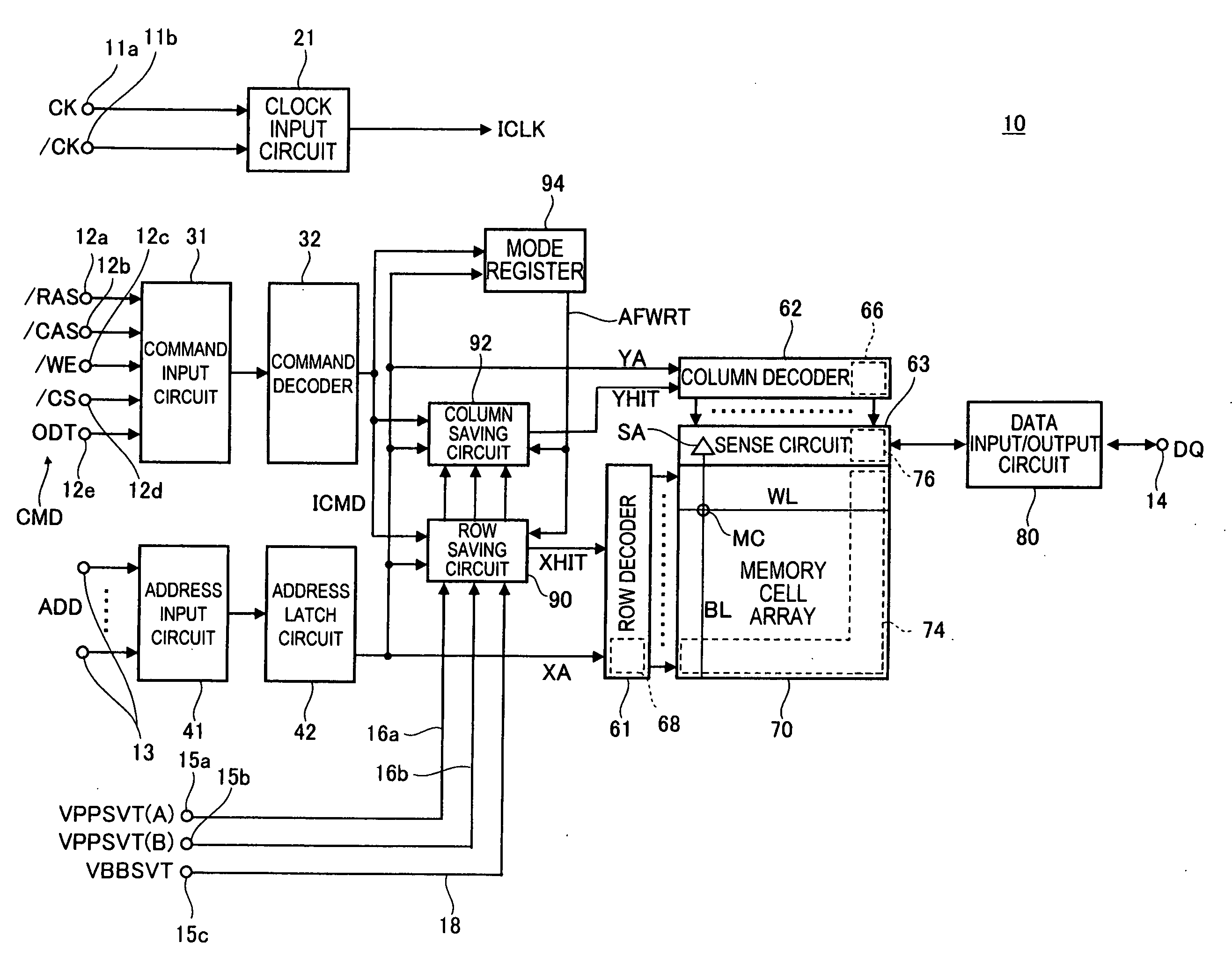
[0033]FIG. 1 is a functional block diagram of a semiconductor memory device 10 according to an embodiment of the present invention. The semiconductor memory device 10 is a DDR (Double-Data-Rate) SDRAM (Synchronous Dynamic Random Access Memory), including clock terminals 11a and 11b, command terminals 12a to 12e, an address terminal 13, a data input / output terminal 14, and power source terminals 15a to 15c, as external terminals. Although the semiconductor memory device 10 further includes a data strobe terminal, a reset terminal, a calibration terminal and the like, these terminals are omitted in FIG. 1.

[0034]The clock terminals 11a and 11b are supplied with external clock signals CK and / CK, respectively. The external clock signals CK and / CK are then supplied to a clock input circuit 21. A signal with “ / ” attached at the head in this specification mean...


PUM


Abstract

A bit memory circuit of an antifuse element set includes two antifuse elements of which logical states are changed from an insulation state to a conductive state when a program voltage is applied. 1-bit data is represented by the logical states of the two antifuse elements. The two antifuse elements are collectively controlled by one decoder circuit. When writing data, the decoder circuit simultaneously performs insulation-breakdown on the two antifuse elements by simultaneously connecting the two antifuse elements to program voltage lines, respectively.

Description

BACKGROUND OF THE INVENTION[0001]1. Field of the Invention[0002]The present invention relates to a semiconductor device, and more particularly to a semiconductor device that stores a defective address by a nonvolatile memory element.[0003]2. Description of Related Art[0004]In a semiconductor memory device such as a DRAM (Dynamic Random Access Memory), the number of memory cells that do not function properly (hereinafter, “defective cells”) increases with an increase of a memory density. To solve this problem, auxiliary memory cells called “redundant cells” are prepared in advance in the semiconductor memory device. By replacing a defective cell with a redundant cell, a memory address of the defective cell (hereinafter, “defective address”) is saved. A detection of the defective cell and a replacement with the redundant cell are performed in a wafer state at a time of manufacturing the semiconductor memory device. Specifically, the defective address is detected at an operation test t...

Claims


Application Information

Patent Timeline
IPC IPC(8): G11C17/16
CPCG11C17/18
Inventor KUBOUCHI, SHUICHIFUJISAWA, HIROKI
Owner LONGITUDE LICENSING LTD
Features
  • Generate Ideas
  • Intellectual Property
  • Life Sciences
  • Materials
  • Tech Scout
  • Unparalleled Data Quality
  • Higher Quality Content
  • 60% Fewer Hallucinations
Learn More