Unlock instant, AI-driven research and patent intelligence for your innovation.

Semiconductor device having ODT function and data processing system including the same

a technology of odt and data processing system, which is applied in the direction of digital storage, instruments, and increasing the degree of modification, can solve the problems of dll circuit stoppage, odt operation not fast enough, and inability to correctly count the latency, so as to prevent the odt operation and reduce the chip area , the effect of circuit scal

Active Publication Date: 2011-03-10
LONGITUDE LICENSING LTD
View PDF7 Cites 10 Cited by
  • Summary
  • Abstract
  • Description
  • Claims
  • Application Information

AI Technical Summary

Benefits of technology

[0014]According to the present invention, when the asynchronous mode shifts to the synchronous mode, the second internal ODT signal having the same logic value as that of the first internal ODT signal at a shifting time is output during a constant period of time. Therefore, an interruption of the ODT operation can be prevented without separately providing a counter that counts a latency of a clock enable signal. Consequently, the circuit scale is reduced, the chip area can be reduced, and the power consumption can be also reduced.

Problems solved by technology

This arrangement is set because when the value of the ODTL is fixed at two clock cycles, a clock frequency improves and a clock cycle becomes short, resulting in a state where ON / OFF of the ODT operation is not quick enough.
When having entered in the slow power-down mode, an operation of a DLL circuit stops because of its reduced power consumption, and its latency cannot be correctly counted.
What is problematic is a case of shifting from a slow power-down mode to a normal mode while an external ODT signal is activated.
Therefore, the circuit scale becomes larger and the power consumption also becomes larger.
The above problems occur not only in DDR3 SDRAMs but also in common in semiconductor devices having a synchronous mode of activating an ODT synchronously with a clock signal and an asynchronous mode of activating an ODT asynchronously with a clock signal.

Method used


Image

  • Semiconductor device having ODT function and data processing system including the same
  • Semiconductor device having ODT function and data processing system including the same
  • Semiconductor device having ODT function and data processing system including the same

Examples


first embodiment

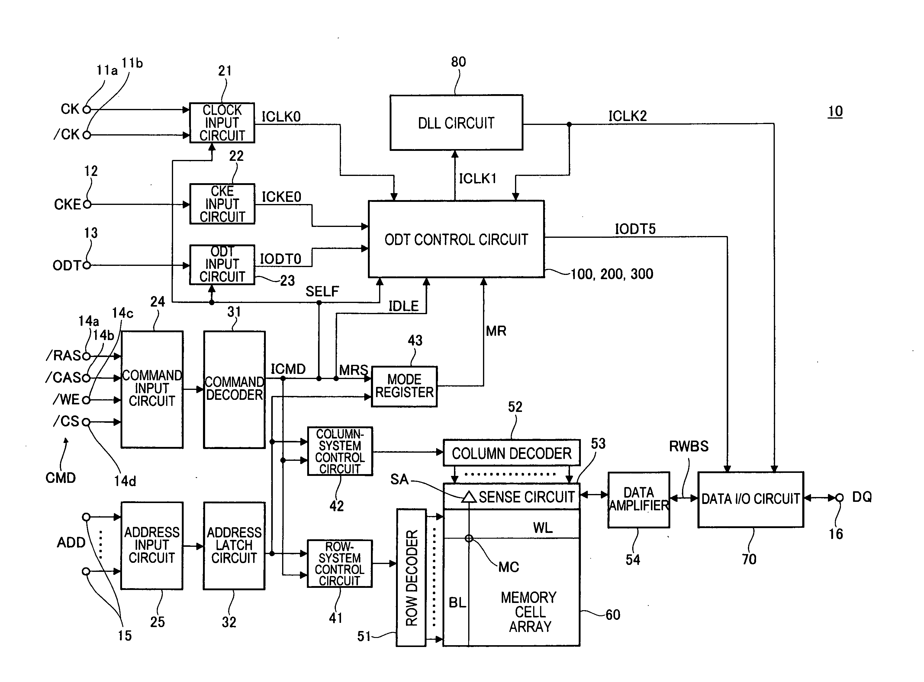
[0039]FIG. 2 is a circuit diagram of the ODT control circuit 100 according to the present invention.

[0040]As shown in FIG. 2, the ODT control circuit 100 includes an ODT latch circuit 101 that latches the internal ODT signal IODT0, and a CKE latch circuit 102 that latches the internal-clock enable signal ICKE0. The latch circuits 101 and 102 perform a latch operation synchronously with the internal clock signal ICLK0. Therefore, an internal ODT signal IODT1 and an internal-clock enable signal ICKE1 as outputs of the latch circuits 101 and 102 respectively become signals synchronous with the internal clock signal ICLK0.

[0041]Further, the ODT control circuit 100 further includes an AL counter 110 that receives the internal ODT signal IODT1 output from the latch circuit 101, counts the internal clock signal ICLK0 by an additive latency, and outputs an internal ODT signal IODT3. The AL counter 110 is what is called a FIFO counter, and sequentially outputs the internal ODT signal IODT1 s...

second embodiment

[0064]The ODT control circuit 200 according to the present invention is explained next.

[0065]FIG. 5 is a circuit diagram of the ODT control circuit 200 according to the second embodiment. The ODT control circuit 200 according to the second embodiment can be used instead of the ODT control circuit 100 shown in FIG. 2.

[0066]As shown in FIG. 5, the ODT control circuit 200 does not include the CWL counters 103 and 105 and the multiplexer 104 included in the ODT control circuit 100, and includes a CWL counter 201 instead. Further, the ODT control circuit 200 includes a delay circuit 202 of which a delay amount is tXPDLL, instead of the delay circuit 107. The ODT control circuit 200 is the same as the ODT control circuit 100 in other features. Therefore, like reference numerals are denoted to like constituent elements and redundant explanations thereof will be omitted.

[0067]The CWL counter 201 has a function same as that of the CWL counter 103, and has a function of setting all contents o...

third embodiment

[0075]The ODT control circuit 300 according to the present invention is explained next.

[0076]FIG. 7 is a circuit diagram of the ODT control circuit 300 according to the third embodiment. The ODT control circuit 300 according to the third embodiment can be used instead of the ODT control circuit 100 shown in FIG. 2 or instead of the ODT control circuit 200 shown in FIG. 5.

[0077]As shown in FIG. 7, the ODT control circuit 300 includes an ODT latch circuit 301 and a CKE latch circuit 302 instead of the ODT latch circuit 101 and the CKE latch circuit 102 included in the ODT control circuit 200. Further, the ODT control circuit 300 includes an OR gate 303 instead of the AND gate 106. The ODT control circuit 300 is the same as the ODT control circuit 200 in other constituent elements. Therefore, like reference numerals are denoted to like constituent elements and redundant explanations thereof will be omitted.

[0078]The OR gate 303 is supplied with a self refresh signal SELF and the power ...


PUM


Abstract

To include an AL counter that outputs a second ODT signal after counting a clock signal by an additive latency after receiving a first ODT signal, and a counter control circuit that controls the AL counter such that the second ODT signal having the same logic value as a logic value of the first ODT signal at a time of shifting from an asynchronous mode to a synchronous mode is output during a period until when at least the clock signal is input by an additive latency after the shifting. With this configuration, an interruption of an CDT operation can be prevented without separately providing a CKE counter. Therefore, the circuit scale can be reduced and the power consumption can be also reduced.

Description

BACKGROUND OF THE INVENTION[0001]1. Field of the Invention[0002]The present invention relates to a semiconductor device and a data processing system including the same, and more particularly relates to a semiconductor device having an ODT (On Die Termination) function and a data processing system including the semiconductor device.[0003]2. Description of Related Art[0004]In a semiconductor device having plural chips arranged in parallel on an external bus, such as a DRAM (Dynamic Random Access Memory), a signal is occasionally reflected by chips having an output buffer in a high impedance state (Hi-Z). The signal quality on the external bus is degraded when such a reflection of a signal occurs. Therefore, a semiconductor device required to have a high data-transfer rate, such as a DDR2 SDRAM or a DDR3 SDRAM (Synchronous DRAM), often includes an ODT function that causes an output circuit to function as a terminating resistor.[0005]When a semiconductor device has an ODT function, a te...

Claims


Application Information

Patent Timeline
IPC IPC(8): G11C8/18H03K19/003
CPCG11C5/063G11C7/222G11C7/1057G11C7/1051
Inventor FUJISAWA, HIROKI
Owner LONGITUDE LICENSING LTD