Method for Fabricating a Micromirror with Self-Aligned Actuators

a self-aligning actuator and micro-mirror technology, applied in the field of optical scanning devices, can solve the problems of inability to accurately adjust the self-alignment procedure, and inability to achieve perfect linear transformation between input voltage and mechanical scan angl

Inactive Publication Date: 2011-03-17
BOARD OF RGT THE UNIV OF TEXAS SYST
View PDF4 Cites 6 Cited by
  • Summary
  • Abstract
  • Description
  • Claims
  • Application Information

AI Technical Summary

Benefits of technology

[0007]In accordance with a preferred embodiment of the present invention, a set of coarse features is initially formed in a low-temperature oxide (LTO) layer deposited on a front side of a wafer. The wafer includes a substrate, a first and second silicon device layers separated from each other by a first and second silicon dioxide layers. A set of fine features is then formed in a photosensitive material layer deposited on top of the LTO layer, and the fine features are constrained late

Problems solved by technology

Conventional electrostatic combdriven micromirrors do not offer perfect linear transformation between input voltages and mechanical scan angles.
In addition, conventional

Method used


Image

  • Method for Fabricating a Micromirror with Self-Aligned Actuators
  • Method for Fabricating a Micromirror with Self-Aligned Actuators
  • Method for Fabricating a Micromirror with Self-Aligned Actuators

Examples


Embodiment Construction

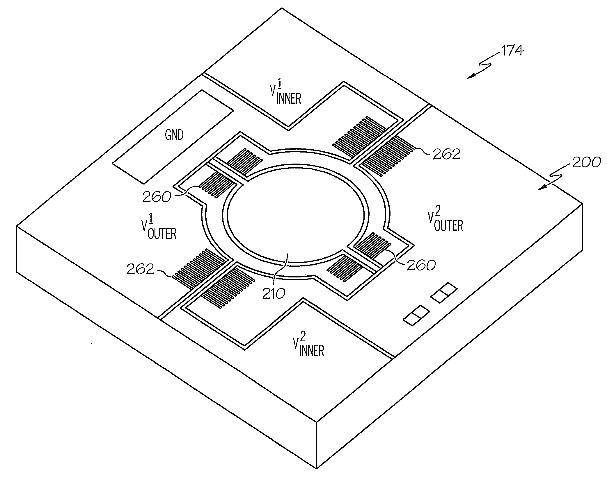
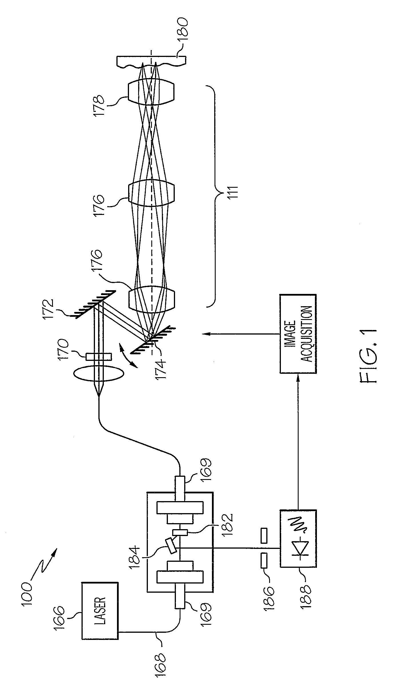
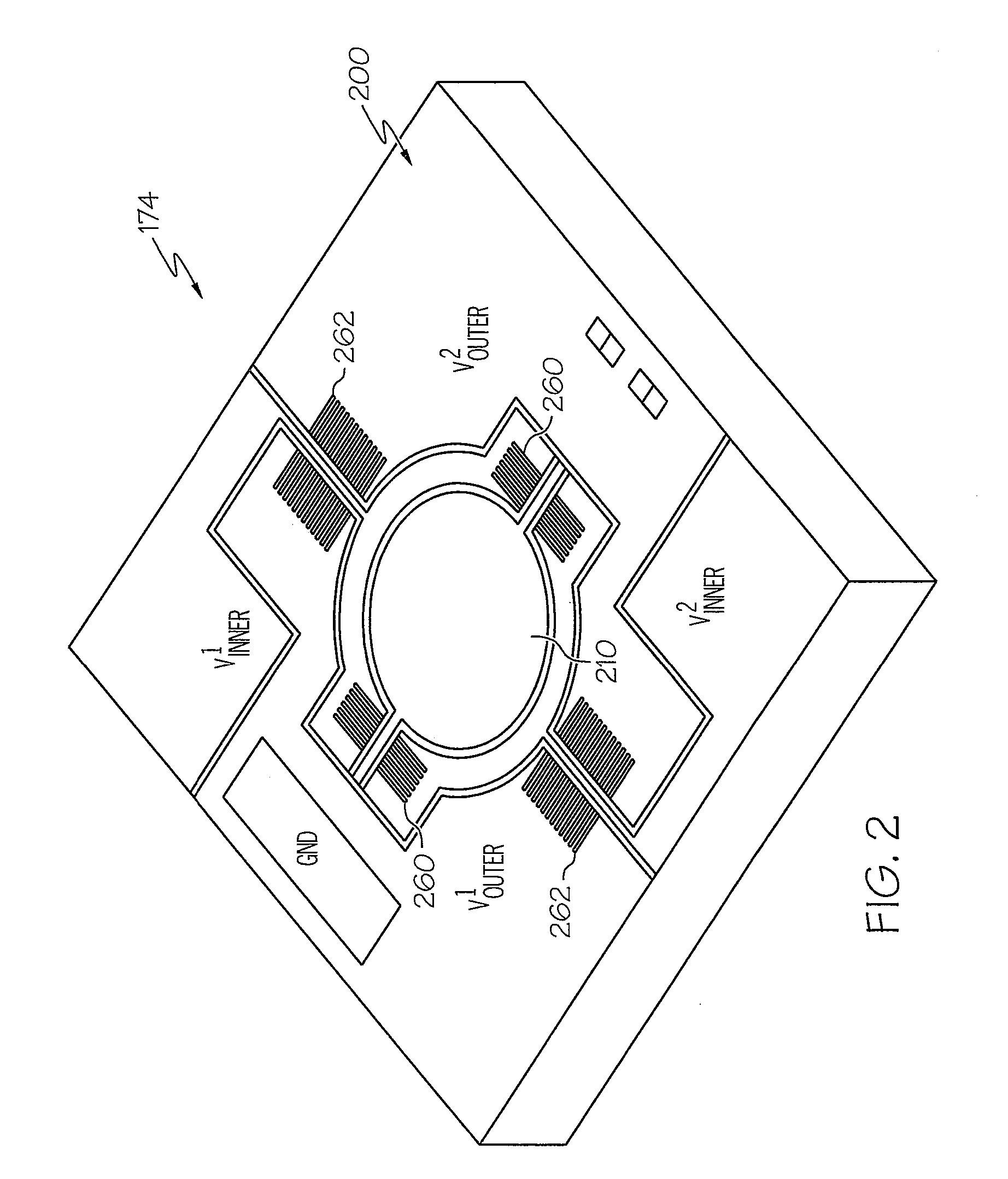
[0014]Referring now to the drawings and in particular to FIG. 1, there is depicted a diagram of a laser-scanning confocal microscope in which a preferred embodiment of the present invention is applicable. As shown, a laser-scanning confocal microscope 100 includes a diode laser 166, an avalanche photodetector 188, a stationary mirror 172, a movable micromirror 174 and an objective system 111 having a 3× Keplerian beam expander 176 and a high-numerical aperture aspheric objective lens 178.

[0015]A linearly-polarized laser beam from diode laser 166 is initially coupled into a single-mode polarization maintaining (PM) fiber 168. Light exiting PM fiber 168 is then collimated by collimators 169 to a 1 mm diameter beam through a zero-order quarter wave-plate 170 whose axis is oriented at 45° to the incident polarization angle in order to convert the illumination to a circular polarization. After reflection off stationary mirror 172, the illumination is incident on micromirror 174 at 22.5° ...


PUM


Abstract

A method of fabricating a micromirror is disclosed. Initially, a set of coarse features is formed in a low-temperature oxide (LTO) layer deposited on a front side of a wafer. A set of fine features is then formed in a photosensitive material layer deposited on top of the LTO layer, and the fine features are constrained laterally within the coarse features. Next, a portion of the LTO layer is removed to align the width of the coarse features with the width of the fine features. The first silicon dioxide layer and the first and second silicon device layers are subsequently etched to form stator comb fingers and rotor comb fingers. Finally, a rotatable mirror is formed by removing a portion of the substrate on a back side of the wafer, and the silicon dioxide layers from the front and back sides of the wafer.

Description

PRIORITY CLAIM[0001]The present application claims priority under 35 U.S.C. §119(e)(1) to provisional application No. 61 / 243,012 filed on Sep. 16, 2009, the contents of which are incorporated herein by reference.BACKGROUND OF THE INVENTION[0002]1. Technical Field[0003]The present invention relates to optical scanning devices in general, and in particular to a method for fabricating micromirrors to be utilized in optical scanning devices.[0004]2. Description of Related Art[0005]Conventional electrostatic combdriven micromirrors do not offer perfect linear transformation between input voltages and mechanical scan angles. In addition, conventional electrostatic combdriven micromirrors often experience scanning instabilities due to pull-in phenomena. Thus, self-alignment procedures have been adopted in the micromirror fabrication process in order to mitigate the above-mentioned problems. However, such self-alignment procedures can be overly complicated.[0006]Consequently, it would be de...

Claims


Application Information

Patent Timeline
IPC IPC(8): B29D11/00
CPCG02B26/0841B29D11/00596
Inventor KUMAR, KARTHIKZHANG, XIAOJING
Owner BOARD OF RGT THE UNIV OF TEXAS SYST
Why Eureka
Try Eureka