Semiconductor device and manufacturing method thereof

a technology of semiconductors and semiconductors, applied in the direction of semiconductor devices, basic electric elements, electrical equipment, etc., can solve the problems of power consumption affecting the continuous operation time, and achieve the effects of low power consumption, low power consumption, and low parasitic capacitan

Inactive Publication Date: 2011-03-17
SEMICON ENERGY LAB CO LTD
View PDF131 Cites 186 Cited by
  • Summary
  • Abstract
  • Description
  • Claims
  • Application Information

AI Technical Summary

Benefits of technology

[0050]A semiconductor device with less parasitic capacitance and low power consumption can be provided as a semiconductor device including a thin film transistor using an oxide semiconductor layer.
[0051]A semiconductor device with high reliability can be provided as a semiconductor device including a thin film transistor using an oxide semiconductor layer.

Problems solved by technology

Power consumption that affects the continuous operation time is a serious concern for such a mobile electronic device.

Method used


Image

  • Semiconductor device and manufacturing method thereof
  • Semiconductor device and manufacturing method thereof
  • Semiconductor device and manufacturing method thereof

Examples


embodiment 1

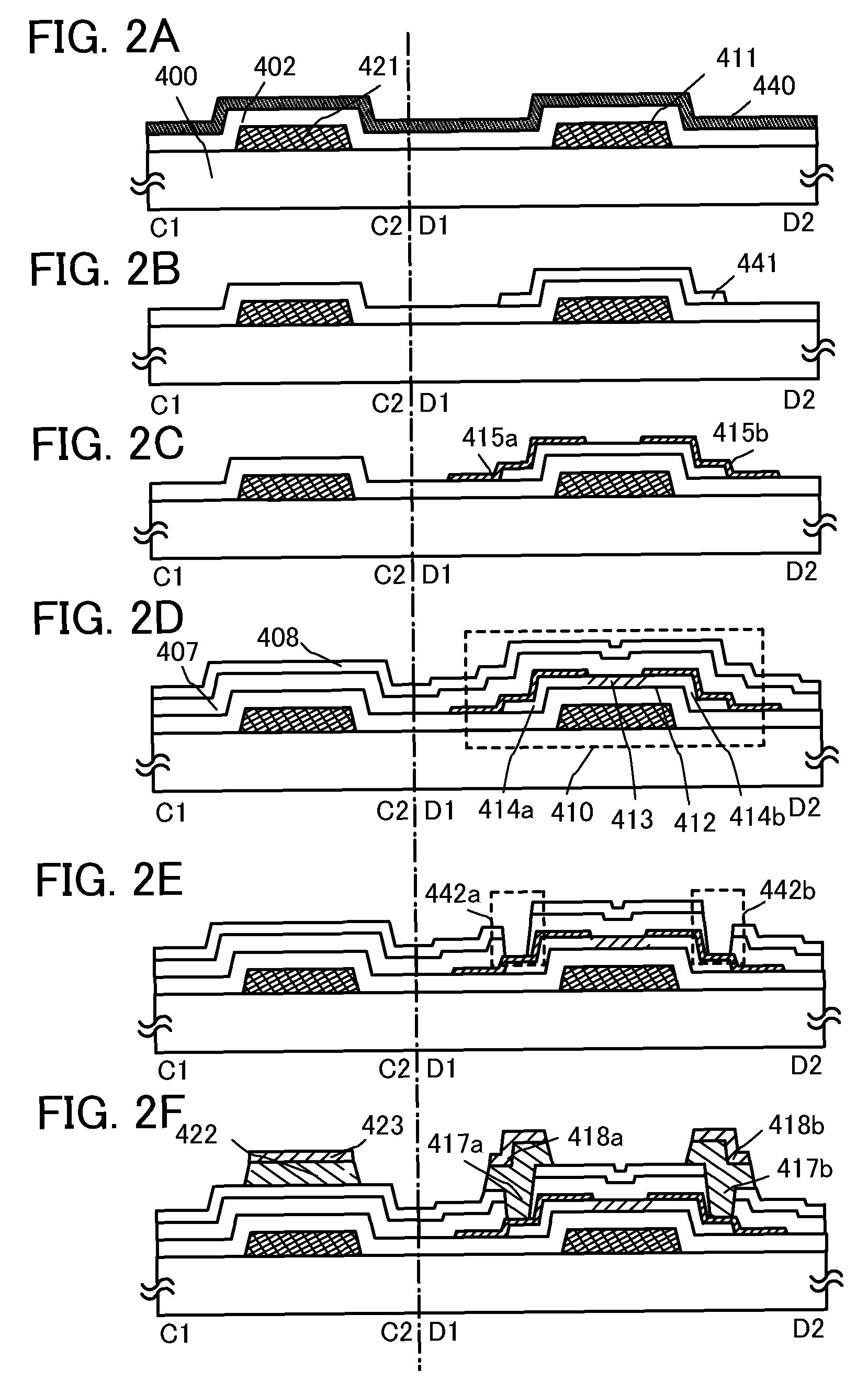
[0080]In Embodiment 1, one embodiment of a semiconductor device and a manufacturing method of the semiconductor device will be described with reference to FIGS. 1A1 and 1A2 and FIG. 1B, FIGS. 2A to 2F, and FIGS. 6A and 6B.

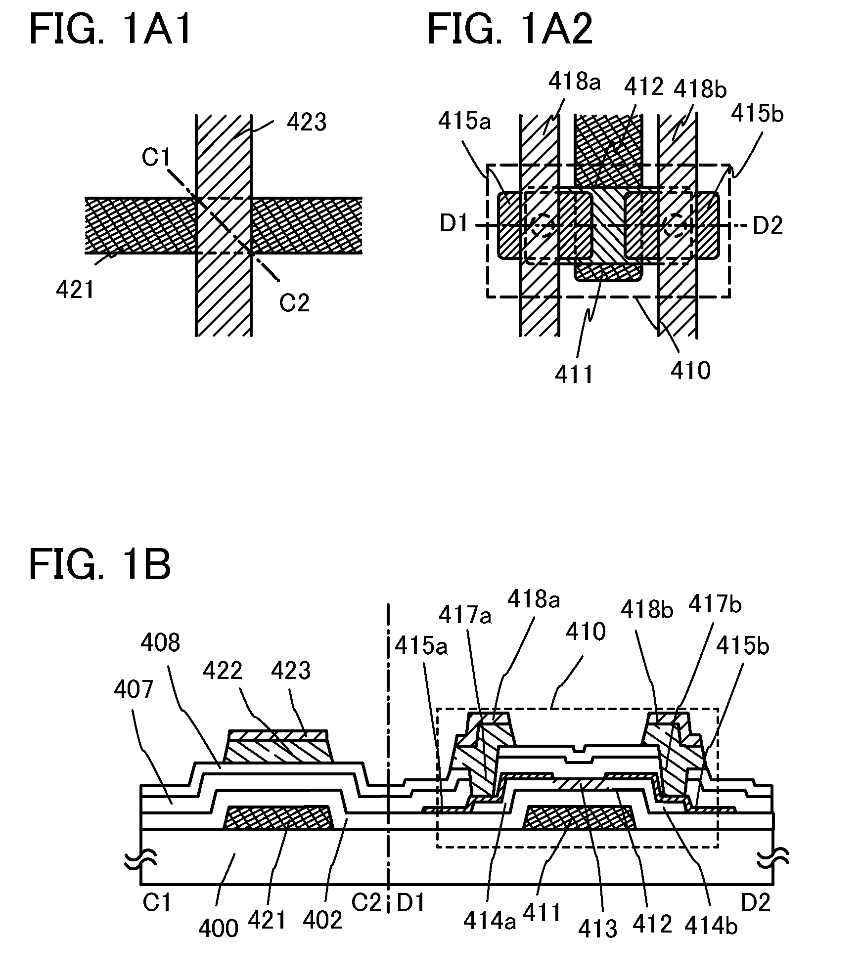
[0081]FIGS. 1A1 and 1A2 illustrate an example of a plane surface structure of a semiconductor device, and FIG. 1B illustrates an example of a cross-sectional structure of the same. A thin film transistor 410 shown in FIGS. 1A2 and 1B is a kind of bottom-gate structure called a channel-etched type and is also called an inverted staggered thin film transistor.

[0082]FIG. 1A1 is a plane view of an intersection between a gate wiring layer (formed by the same step as a gate electrode layer) and a source wiring layer (formed by the same step as a wiring layer); FIG. 1A2 is a plane view of the channel-etched thin film transistor 410; and FIG. 1B is a cross-sectional view along line C1-C2 and line D1-D2 in FIGS. 1A1 and 1A2.

[0083]The thin film transistor 410, which is a cha...

embodiment 2

[0167]In Embodiment 2, an example of a semiconductor device including a thin film transistor having a structure different from that of Embodiment 1 will be described below.

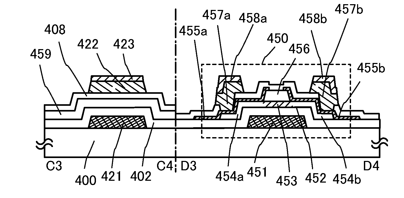
[0168]FIGS. 3A1 and 3A2 illustrate an example of a plane surface structure of a semiconductor device, and FIG. 3B illustrates an example of a cross-sectional structure of the same. A thin film transistor 450 shown in FIGS. 3A2 and 3B is a kind of bottom-gate structure called a channel-protective type (channel-stop type) and is also called an inverted staggered thin film transistor.

[0169]FIG. 3A1 is a plane view of an intersection between a gate wiring layer (formed by the same step as a gate electrode layer) and a source wiring layer (formed by the same step as a wiring layer); FIG. 3A2 is a plane view of the channel-protective type thin film transistor 450; and FIG. 3B is a cross-sectional view along line C3-C4 and line D3-D4 in FIGS. 3A1 and 3A2.

[0170]The thin film transistor 450, which is a channel-protective t...

embodiment 3

[0208]In Embodiment 3, another example which is different from Embodiment 1 in the manufacturing process of a semiconductor device including a thin film transistor will be described with reference to FIGS. 5A to 5F. FIGS. 5A to 5F are the same as FIGS. 1A1, 1A2, and FIG. 1B and FIGS. 2A to 2F except that there is a difference in part of the process; therefore, the same portions are denoted by the same reference numerals, and detailed description of the same portions is omitted. In this embodiment, a mask layer formed using a multi-tone mask is used in a photolithography step.

[0209]Since a mask layer formed with the use of a multi-tone mask has a plurality of film thicknesses and further can be changed in shape by performing etching on the mask layer, the mask layer can be used in a plurality of etching steps for processing into different patterns. Therefore, a mask layer corresponding at least two kinds of different patterns can be formed by one multi-tone mask. Thus, the number of ...


PUM


Abstract

It is an object to provide a semiconductor device with less power consumption as a semiconductor device including a thin film transistor using an oxide semiconductor layer. It is an object to provide a semiconductor device with high reliability as a semiconductor device including a thin film transistor using an oxide semiconductor layer. In the semiconductor device, a gate electrode layer (a gate wiring layer) intersects with a wiring layer which is electrically connected to a source electrode layer or a drain electrode layer with an insulating layer which covers the oxide semiconductor layer of the thin film transistor and a gate insulating layer interposed therebetween. Accordingly, the parasitic capacitance formed by a stacked-layer structure of the gate electrode layer, the gate insulating layer, and the source or drain electrode layer can be reduced, so that low power consumption of the semiconductor device can be realized.

Description

TECHNICAL FIELD[0001]The present invention relates to a semiconductor device including an oxide semiconductor and a manufacturing method thereof.[0002]In this specification, a semiconductor device means any device which can function by utilizing semiconductor characteristics; an electrooptical device, a semiconductor circuit, and an electronic appliance are all semiconductor devices.BACKGROUND ART[0003]In recent years, a technique for forming a thin film transistor (TFT) by using a semiconductor thin film (having a thickness of about several nanometers to several hundred nanometers) formed over a substrate having an insulating surface has attracted attention. Thin film transistors are applied to a wide range of electronic devices such as ICs or electrooptical devices, and particularly, prompt development of thin film transistors that are to be used as switching elements in image display devices is being pushed. Various metal oxides are used for a variety of applications. Indium oxid...

Claims


Application Information

Patent Timeline
Patent Type & Authority Applications(United States)
IPC IPC(8): H01L29/12H01L21/16
CPCH01L27/1225H01L29/7869H01L2924/0002H01L2924/00H01L29/78606H01L27/1214H01L33/36H01L33/62
Inventor YAMAZAKI, SHUNPEI
Owner SEMICON ENERGY LAB CO LTD
Why Eureka
Try Eureka