Epitaxial substrate for semiconductor device, schottky junction structure, and leakage current suppression method for schottky junction structure

a technology of schottky junction and epitaxial substrate, which is applied in the direction of basic electric elements, electrical apparatus, semiconductor devices, etc., to achieve excellent reliability in reverse characteristics of schottky junction

Active Publication Date: 2011-03-17
NGK INSULATORS LTD
View PDF6 Cites 4 Cited by
  • Summary
  • Abstract
  • Description
  • Claims
  • Application Information

AI Technical Summary

Benefits of technology

[0012]According to the present invention, it is possible to obtain a semiconductor device having excellent reliability in reverse characteristics of schottky junction.
[0013]Therefore, an object of the present invention is to provide an epitaxial substrate for semiconductor device that is capable of achieving a semiconductor device having excellent reliability in reverse characteristics of schottky junction.

Problems solved by technology

In order to put the above-mentioned HEMT device or a substrate for HEMT device that is a multi-layer structure used in manufacturing the same to practical use, various problems need to be solved; problems related to performance improvement such as increase of power density and efficiency, problems related to functional improvement such as achieving normally-off operation, and fundamental problems such as enhancing reliability and reducing cost.
One of the above-mentioned problems is to improve schottky junction characteristics.

Method used


Image

  • Epitaxial substrate for semiconductor device, schottky junction structure, and leakage current suppression method for schottky junction structure
  • Epitaxial substrate for semiconductor device, schottky junction structure, and leakage current suppression method for schottky junction structure
  • Epitaxial substrate for semiconductor device, schottky junction structure, and leakage current suppression method for schottky junction structure

Examples


Embodiment Construction

Configuration of Epitaxial Substrate

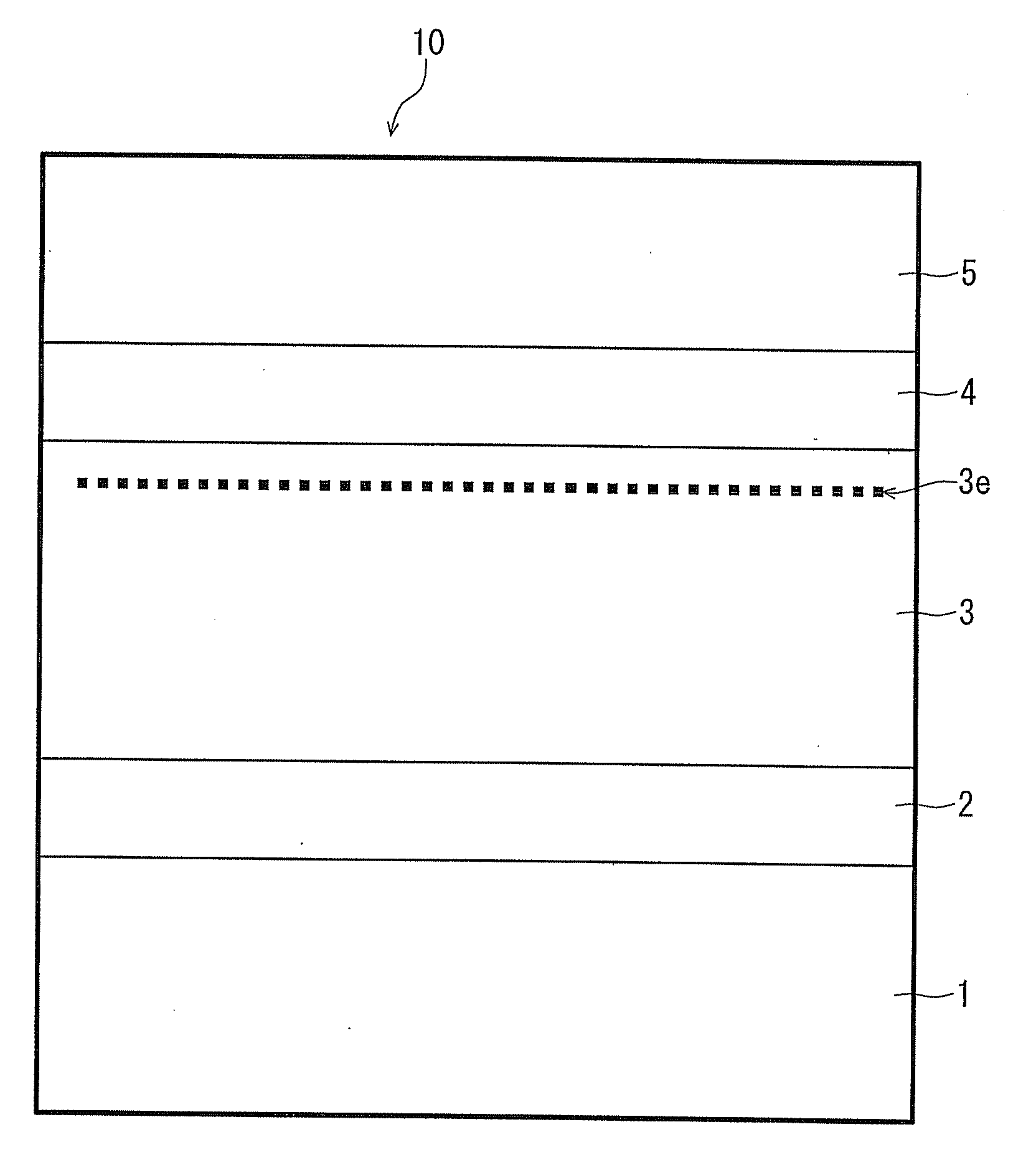
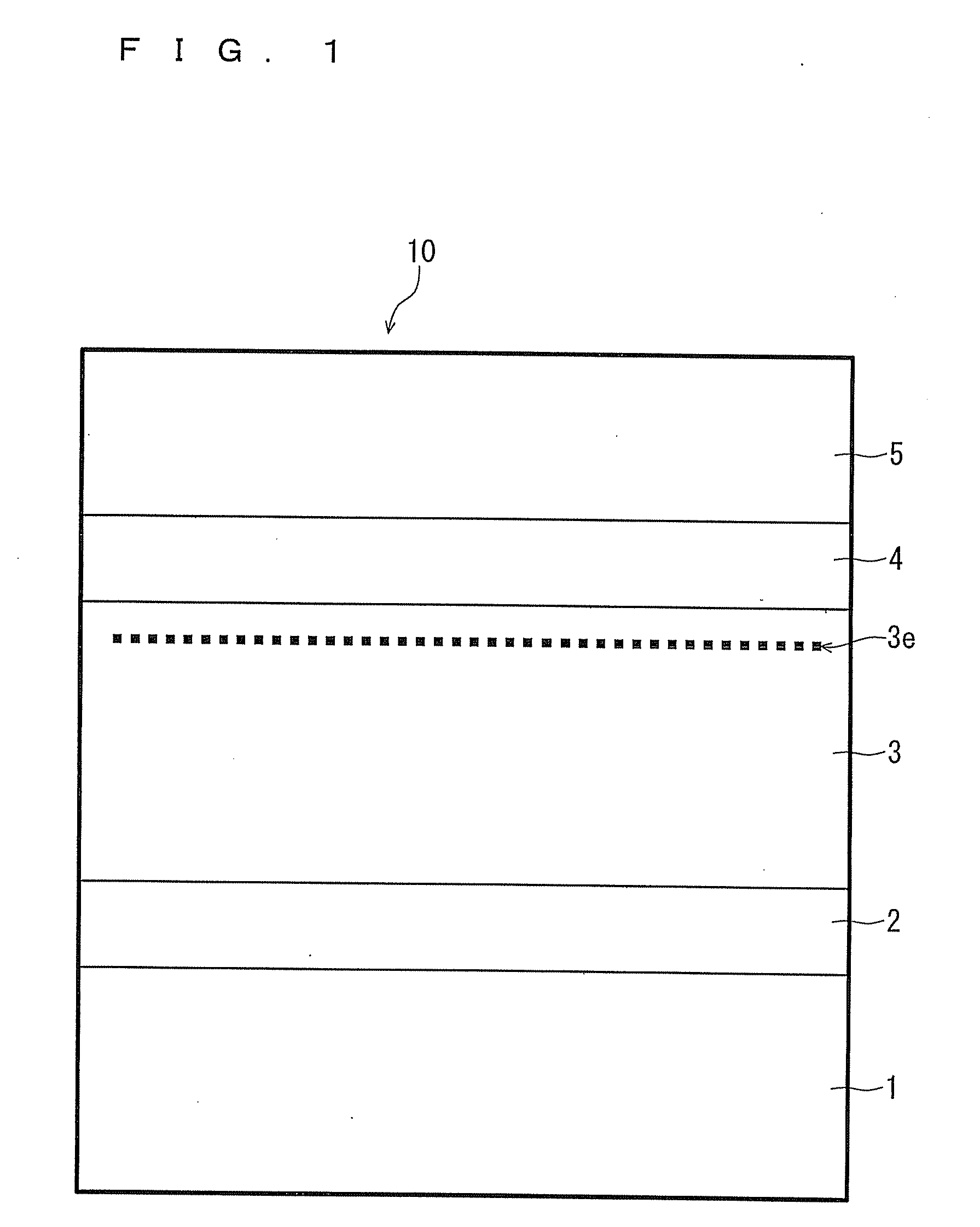
[0017]FIG. 1 is a schematic cross-sectional view schematically showing the configuration of an epitaxial substrate 10 according to a preferred embodiment of the present invention. The epitaxial substrate 10 has the configuration in which a base substrate 1, a buffer layer 2, a channel layer 3, a spacer layer 4 and a barrier layer 5 are formed by lamination. Note that ratios of thickness of the respective layers in FIG. 1 do not reflect actual ones. The buffer layer 2, the channel layer 3, the spacer layer 4 and the barrier layer 5 are preferred examples of layers that are epitaxially formed (details thereof are described below) using the metal organic chemical vapor deposition method (MOCVD method).

[0018]Hereinbelow, while description is given of a case where the MOCVD method is used for the formation of each layer, other epitaxial growth technique, for example, the technique appropriately selected from various vapor phase growth methods and liqui...


PUM


Abstract

Provided is an epitaxial substrate for semiconductor device that is capable of achieving a semiconductor device having high reliability in reverse characteristics of schottky junction. An epitaxial substrate for semiconductor device obtained by forming, on a base substrate, a group of group III nitride layers by lamination such that a (0001) crystal plane of each layer is approximately parallel to a substrate surface includes: a channel layer formed of a first group III nitride having a composition of Inx1Aly1Gaz1N (x1+y1+z1=1, z1>0); and a barrier layer formed of a second group III nitride having a composition of Inx2Aly2N (x2+y2=1, x2>0, y2>0), wherein the second group III nitride is a short-range-ordered mixed crystal having a short-range order parameter α satisfying a range where 0≦α≦1.

Description

BACKGROUND OF THE INVENTION[0001]1. Field of the Invention[0002]The present invention relates to an epitaxial substrate that has a multi-layer structure composed of a group III nitride semiconductor, and more particularly, to a multi-layer structured epitaxial substrate for electronic devices.[0003]2. Description of the Background Art[0004]Nitride semiconductors having high breakdown electric field and high saturation electron velocity have been attracting attention as the next generation of semiconductor materials for high-frequency / high-power devices. For example, a high electron mobility transistor (HEMT) device formed by laminating a barrier layer composed of AlGaN and a channel layer composed of GaN takes advantage of the feature that high-concentration two-dimensional electron gas (2DEG) is generated at a lamination interface (hetero interface) owing to a polarization effect (spontaneous polarization effect and piezo polarization effect) inherent in a nitride material (for exa...

Claims


Application Information

Patent Timeline
Patent Type & Authority Applications(United States)
IPC IPC(8): H01L29/205H01L21/20
CPCH01L21/0237H01L21/02458H01L21/0254H01L29/7787H01L29/045H01L29/2003H01L29/66462H01L21/0262
Inventor MIYOSHI, MAKOTOKURAOKA, YOSHITAKASUMIYA, SHIGEAKIICHIMURA, MIKIYASUGIYAMA, TOMOHIKOTANAKA, MITSUHIRO
Owner NGK INSULATORS LTD
Why Eureka
Try Eureka