Semiconductor device and method for manufacturing the same

a technology of semiconductor devices and manufacturing methods, applied in the field of semiconductor devices, can solve the problems of increasing parasitic resistance, reducing and restricting the selection of processes, so as to reduce the possibility of shortening and reduce the possibility of process defects

Active Publication Date: 2011-03-17
INST OF MICROELECTRONICS CHINESE ACAD OF SCI
View PDF6 Cites 61 Cited by
  • Summary
  • Abstract
  • Description
  • Claims
  • Application Information

AI Technical Summary

Benefits of technology

[0022]In accordance with the present invention, the second source / drain contact hole and the gate contact hole have the same etching depth. Thus, it is possible to effectively reduce the possibilities of shorts occurring between the contact holes and the gate. Moreover, since the etching width / height ratio of the source / drain contact hole and that of the gate contact hole are close to each other, the requirements on etching and the contact hole filling processes are relaxed. At the same time, the possibility of the occurrence of process defects is also reduced. Additionally, the present invention involves the replacement gate process which is compatible with the typical replacement gate procedures.

Problems solved by technology

Fabricating increasingly smaller contacts and contact holes by using conventional processes presents a number of problems.
(2) As an etching depth in the source / drain regions is large whereas a size of openings thereof is small (i.e., it has a small width / height ratio), a number of process defects such as underetch, cavities in metal-filling plugs, and so on may be caused.
Thus, the selection of processes is restricted, and the parasitic resistance increases.

Method used


Image

  • Semiconductor device and method for manufacturing the same
  • Semiconductor device and method for manufacturing the same
  • Semiconductor device and method for manufacturing the same

Examples


Embodiment Construction

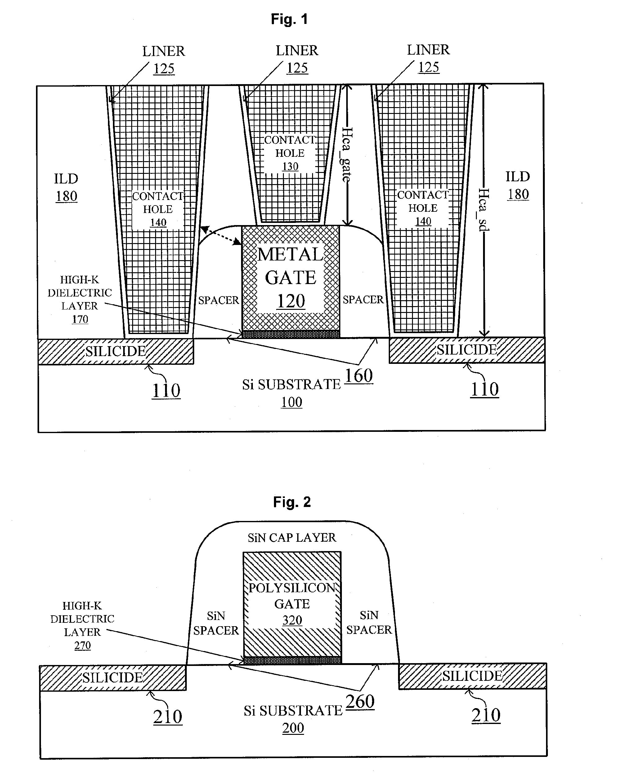
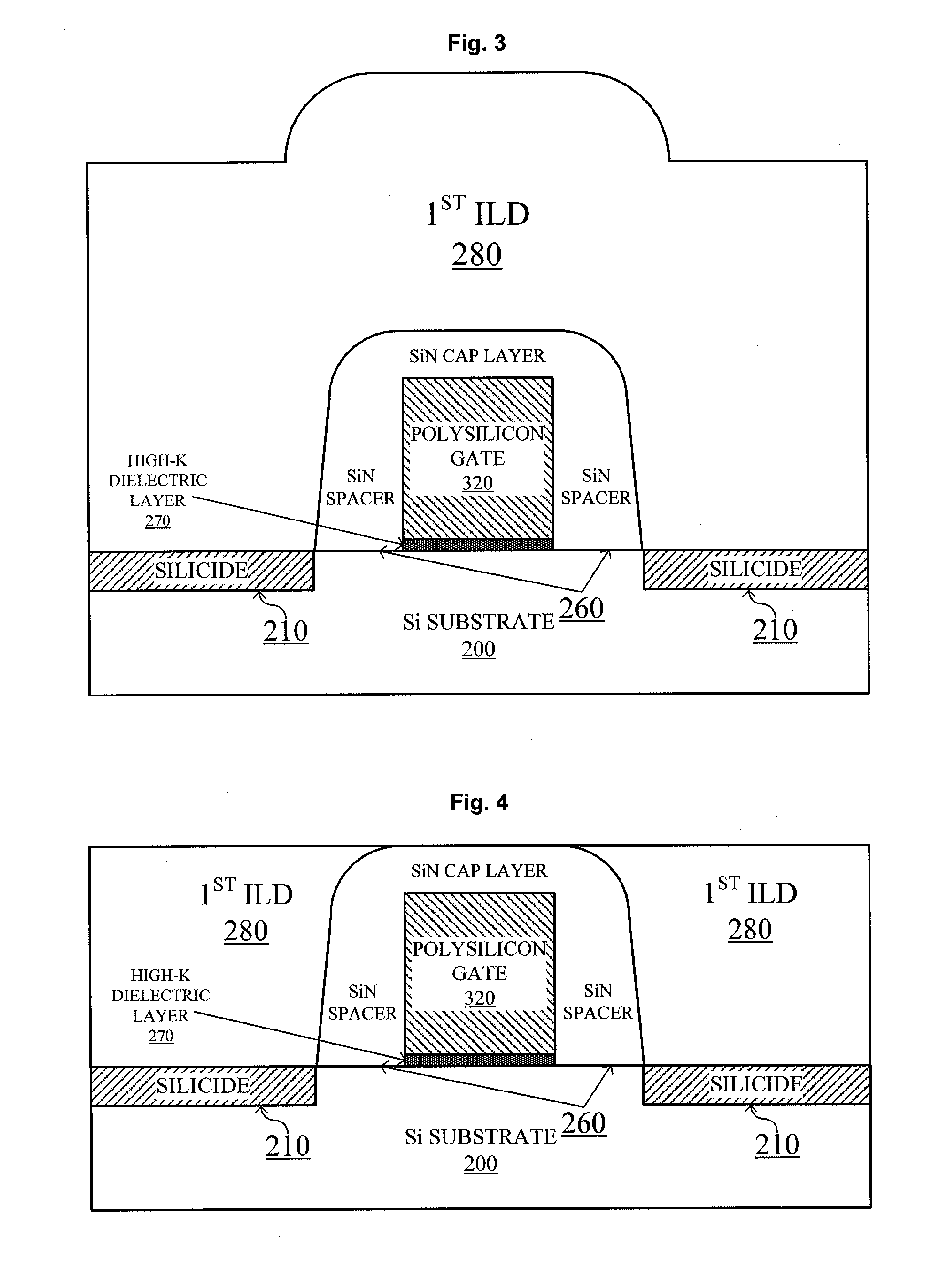
[0027]Hereunder, the present invention will be described in accordance with the drawings. In the following description, while it may blur the understanding of the present invention, the conventional structure or construction will be omitted.

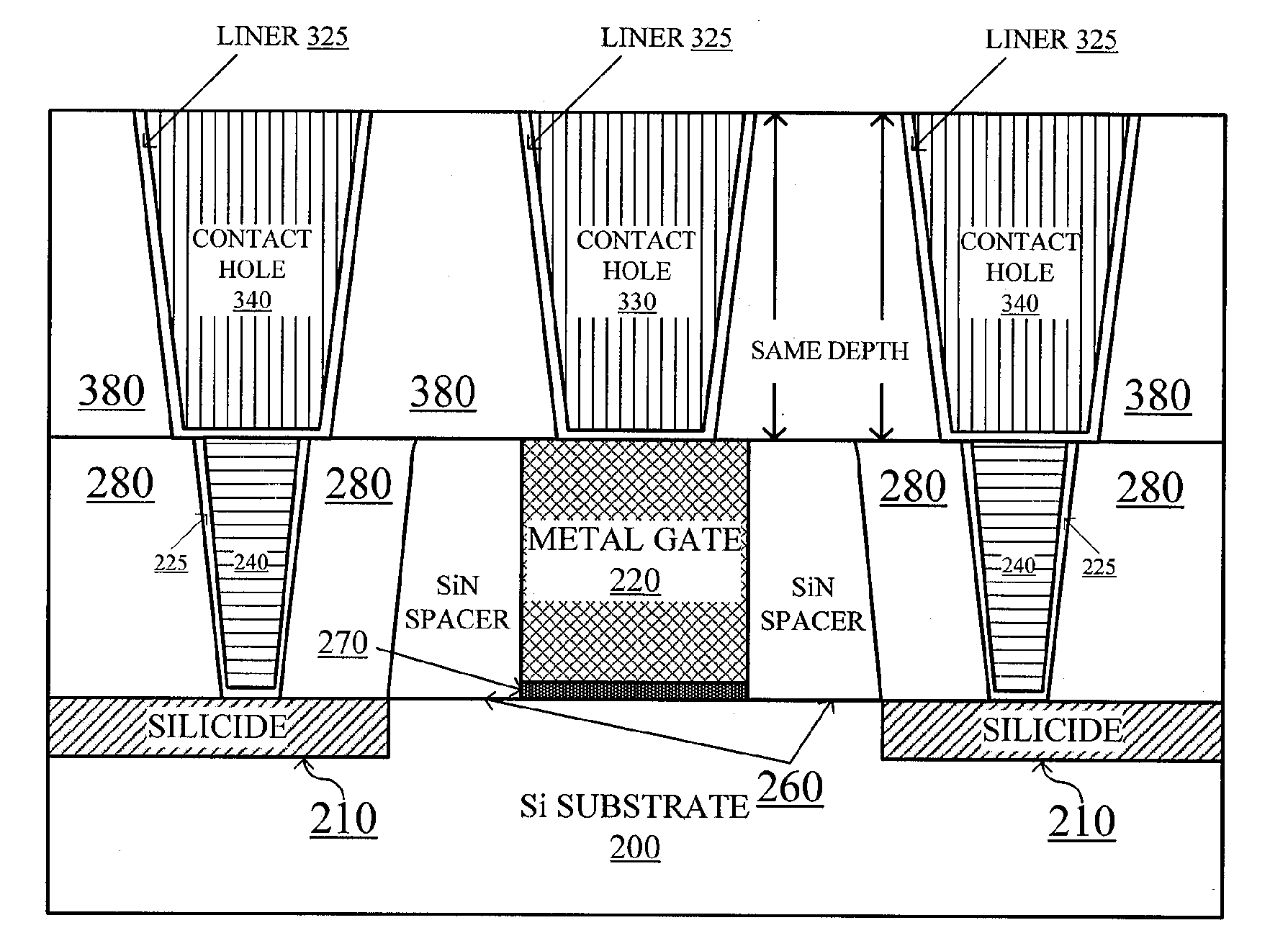
[0028]First of all, by referring to FIG. 14, the semiconductor device manufactured by the inventive process will be described in details. FIG. 14 is a schematic diagram showing a semiconductor device manufactured according to the semiconductor device manufacturing method proposed by the present invention.

[0029]As shown in FIG. 14, the semiconductor device manufactured by the inventive process mainly comprises: a Si substrate 200, a first Inter-Layer Dielectric (ILD) layer 280 (having a thickness of 15-50 nm), a second Inter-Layer Dielectric (ILD) layer 380 (having a thickness of 25-90 nm), silicide regions 210, a metal gate 220, a first source / drain contact holes 240 (having a width of 15-100 nm), a second source / drain contact holes 340 (having a...


PUM


Abstract

The present invention proposes a method of forming a dual contact hole, comprising steps of: forming a source/drain region and a replacement gate structure on a semiconductor substrate, the replacement gate structure including a replacement gate; depositing a first inter-layer dielectric layer; planarizing the first inter-layer dielectric layer to expose the replacement gate in the replacement gate structure; removing the replacement gate and depositing to form a metal gate; etching to form a first source/drain contact opening in the first inter-layer dielectric layer; sequentially depositing a liner and filling conductive metal in the first source/drain contact opening to form a first source/drain contact hole; depositing a second inter-layer dielectric layer on the first inter-layer dielectric layer; etching to form a second source/drain contact opening and a gate contact opening in the second inter-layer dielectric layer; and sequentially depositing a liner and filling conductive metal in the second source/drain contact opening and the gate contact opening to form a second source/drain contact hole and a gate contact hole. The present invention also proposes a semiconductor device manufactured by the above process.

Description

PRIORITY APPLICATION(S)[0001]This patent application claims the benefit of priority, under 35 U.S.C. §119, to Chinese Patent Application Serial Number 200910092514.3, filed Sep. 16, 2009, the entire contents of which are incorporated herein by reference in their entirety.FIELD OF INVENTION[0002]The present invention relates to semiconductor field, especially to semiconductor devices and manufacturing methods thereof, and more particularly, to a method of forming a dual contact hole for replacement gate and a semiconductor device manufactured by means of the method.DESCRIPTION OF PRIOR ART[0003]With the increasingly smaller size of semiconductor device, inter-layer contacts and contact holes (CA) must become smaller, and distances therebetween also become shorter and shorter. Fabricating increasingly smaller contacts and contact holes by using conventional processes presents a number of problems. (1) As an etching depth on gate is different from that in source / drain regions, shorts m...

Claims


Application Information

Patent Timeline
Patent Type & Authority Applications(United States)
IPC IPC(8): H01L29/78H01L21/336
CPCH01L21/76816H01L29/78H01L2924/0002H01L2924/00H01L23/485H01L23/53223H01L23/53238H01L29/517H01L29/66545H01L23/5226H01L23/528H01L29/41H01L21/76838
Inventor YIN, HAIZHOUZHU, HUILONGLUO, ZHIJIONG
Owner INST OF MICROELECTRONICS CHINESE ACAD OF SCI
Why Eureka
Try Eureka