Semiconductor device and a method of fabricating the same

a technology of semiconductor devices and dielectric layers, applied in the direction of semiconductor devices, electrical equipment, transistors, etc., can solve the problems of pipe or seams cannot be completely filled with dielectric layers, etc., and achieve the effect of preventing short circuit between adjacent contact windows

Active Publication Date: 2011-03-17
MACRONIX INT CO LTD
View PDF5 Cites 12 Cited by
  • Summary
  • Abstract
  • Description
  • Claims
  • Application Information

AI Technical Summary

Benefits of technology

[0030]Based on the above, there are no pipes or seams among the stacked gate structures of the semiconductor device according to the present invention, and therefore short circuit of the contact window can be precluded.

Problems solved by technology

As a result, subject to the temperature at which the reflow process is performed, the pipes or the seams can still not be completely filled with the dielectric layer during implementation of the reflow process.
As such, the pipes or the seams are filled with metal deposited in a subsequent process of forming a contact window, thus resulting in short circuit between adjacent contact windows.

Method used


Image

  • Semiconductor device and a method of fabricating the same
  • Semiconductor device and a method of fabricating the same
  • Semiconductor device and a method of fabricating the same

Examples


Embodiment Construction

[0034]In the following descriptions, wordings including “up,”“over,” and “under” serve to indicate reference directions in accompanying figures but not to limit the scope of the present invention. Besides, the word “a” means “at least one” in this disclosure.

[0035]FIGS. 1A through 1F are schematic cross-sectional flowcharts illustrating a method of fabricating a semiconductor device according to an embodiment of the present invention.

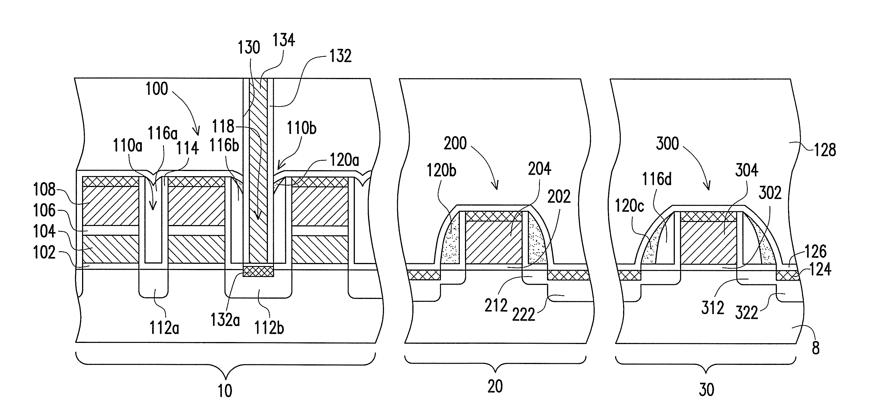
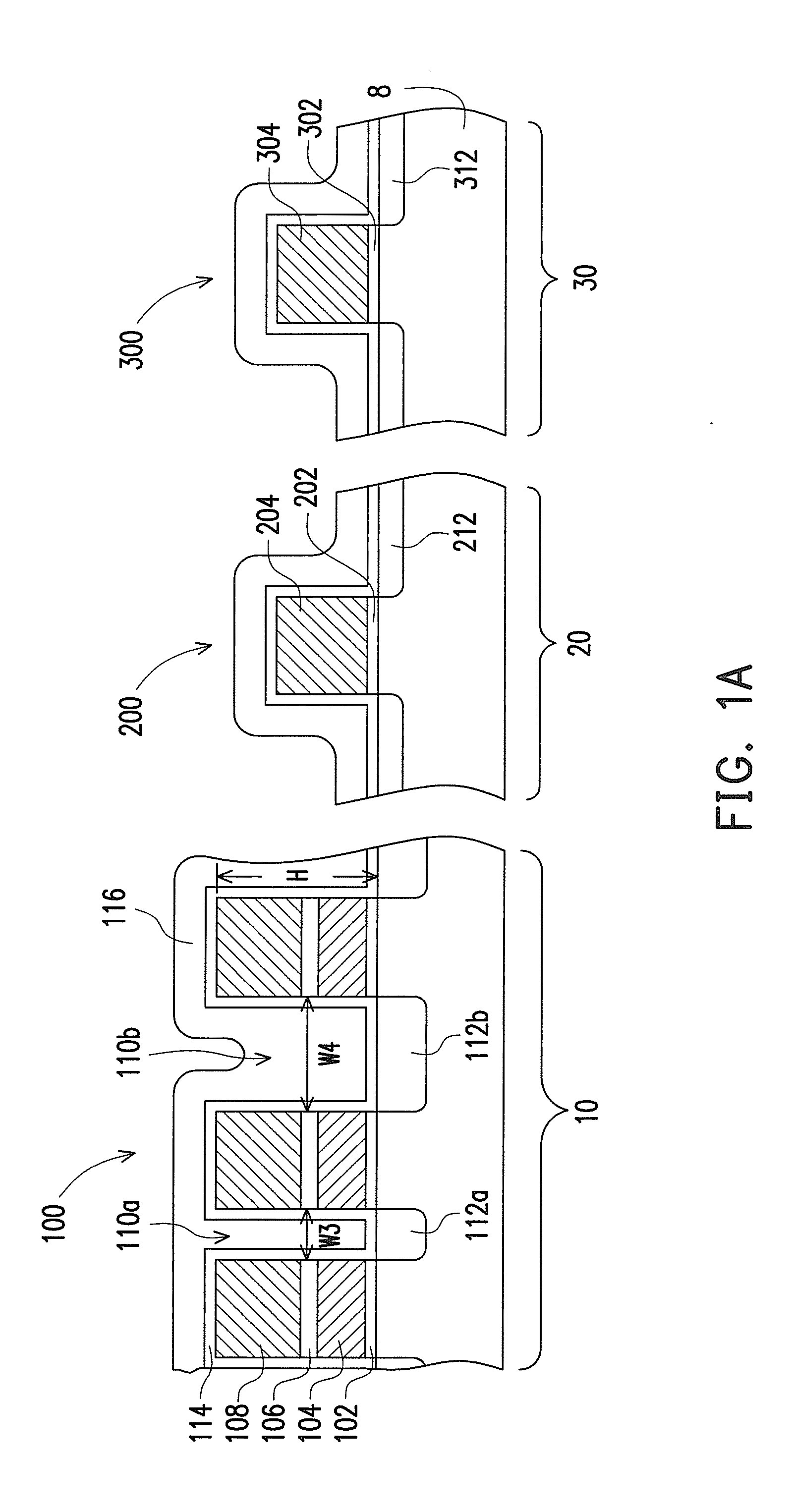
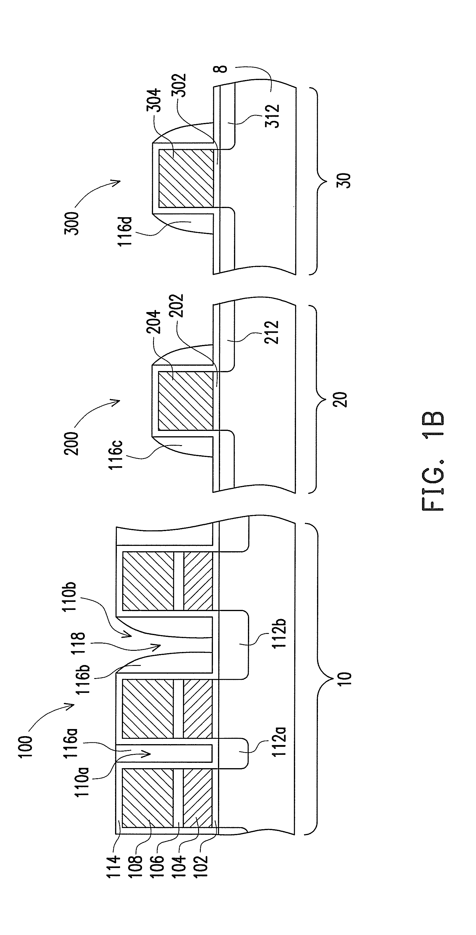
[0036]Referring to FIG. 1A, a substrate 8 is provided. The substrate 8 is, for example, a semiconductor substrate, such as a silicon substrate, a SiGe substrate, or any other appropriate substrate. The substrate 8 includes a first region 10, a second region 20, and a third region 30. In an embodiment, the first region 10 is, for example, a memory cell region, the second region 20 is a first logic circuit region for forming a low voltage device, and the third region 30 is a second logic circuit region for forming a high voltage device.

[0037]A plurality o...


PUM


Abstract

A semiconductor device is provided. The semiconductor device includes a memory device, and the memory device includes a substrate, two stacked gates, two spacers, an insulating layer, and a dielectric layer. The stacked gates having a gap therebetween are located on the substrate. The spacers having a pipe or a seam therebetween are respectively located at sidewalls of each of the stacked gates in the gap. The pipe or the seam is filled with the insulating layer. The dielectric layer is located on the substrate and covers the insulating layer and the stacked gates.

Description

BACKGROUND OF THE INVENTION[0001]1. Field of the Invention[0002]The present invention relates to an integrated circuit and a method of fabricating the same, and more particularly, to a semiconductor device and a method of fabricating the same.[0003]2. Description of Related Art[0004]Memory, so to speak, is a semiconductor device for storing data or information. Among various memory products, a non-volatile memory is characterized by storing, reading, or erasing data repeatedly without loss of data after termination of power supply. Hence, the non-volatile memory has become the semiconductor device extensively applied in personal computers or electronic equipment. In a variety of non-volatile memories, a flash memory possesses advantages of high-speed reading and writing capacity, high memory storage density, and so on. Therefore, the flash memory is applied to communication industry, consumer electronics industry, data processing industry, transportation industry, and so forth.[0005...

Claims


Application Information

Patent Timeline
Patent Type & Authority Applications(United States)
IPC IPC(8): H01L29/788
CPCH01L21/823418H01L21/823468H01L29/66825H01L27/11546H01L27/11526H10B41/49H10B41/40
Inventor WU, TIN-WEIYIH, CHENG-MINGYANG, CHIH-HSIANG
Owner MACRONIX INT CO LTD
Why Eureka
Try Eureka