Semiconductor device and method of manufacturing the same

Active Publication Date: 2011-03-17
MITSUBISHI ELECTRIC CORP
View PDF4 Cites 19 Cited by
  • Summary
  • Abstract
  • Description
  • Claims
  • Application Information

AI Technical Summary

Benefits of technology

[0012]First, a semiconductor layer having a single-crystalline structure is prepared. First and second trenches penetrating the semiconductor layer are formed such that the first and second channel surfaces are formed, respectively. The first channel surface has a first plane orientation, and the second channel surface has a second plane orientation different from the first plane orientation. First and second gate insulating films covering the first and second channel surfaces, respectively, are formed by chemical combination reaction on the first and second channel surfaces. A first gate electrode is formed on the first gate insulating film to fill the first trench, and a second gate electrode is formed on the second gate insulating film to fill the second trench. In the step of forming the first and second trenches, the first and second plane orientations are selected such that a rate of progress of the chemical combination reaction in the second plane orientation of the semiconductor layer is faster than a rate of progress of the chemical combination reaction in the first plane orientation of the semiconductor layer.
[0013]According to the present invention, the thickness of the second gate insulating film is made larger than th

Problems solved by technology

According to the technique in the publication described above, however, in order to obtain a structure in which the voltage threshold value of the sense IGBT cells is higher than the voltage th

Method used


Image

  • Semiconductor device and method of manufacturing the same
  • Semiconductor device and method of manufacturing the same
  • Semiconductor device and method of manufacturing the same

Examples


first embodiment

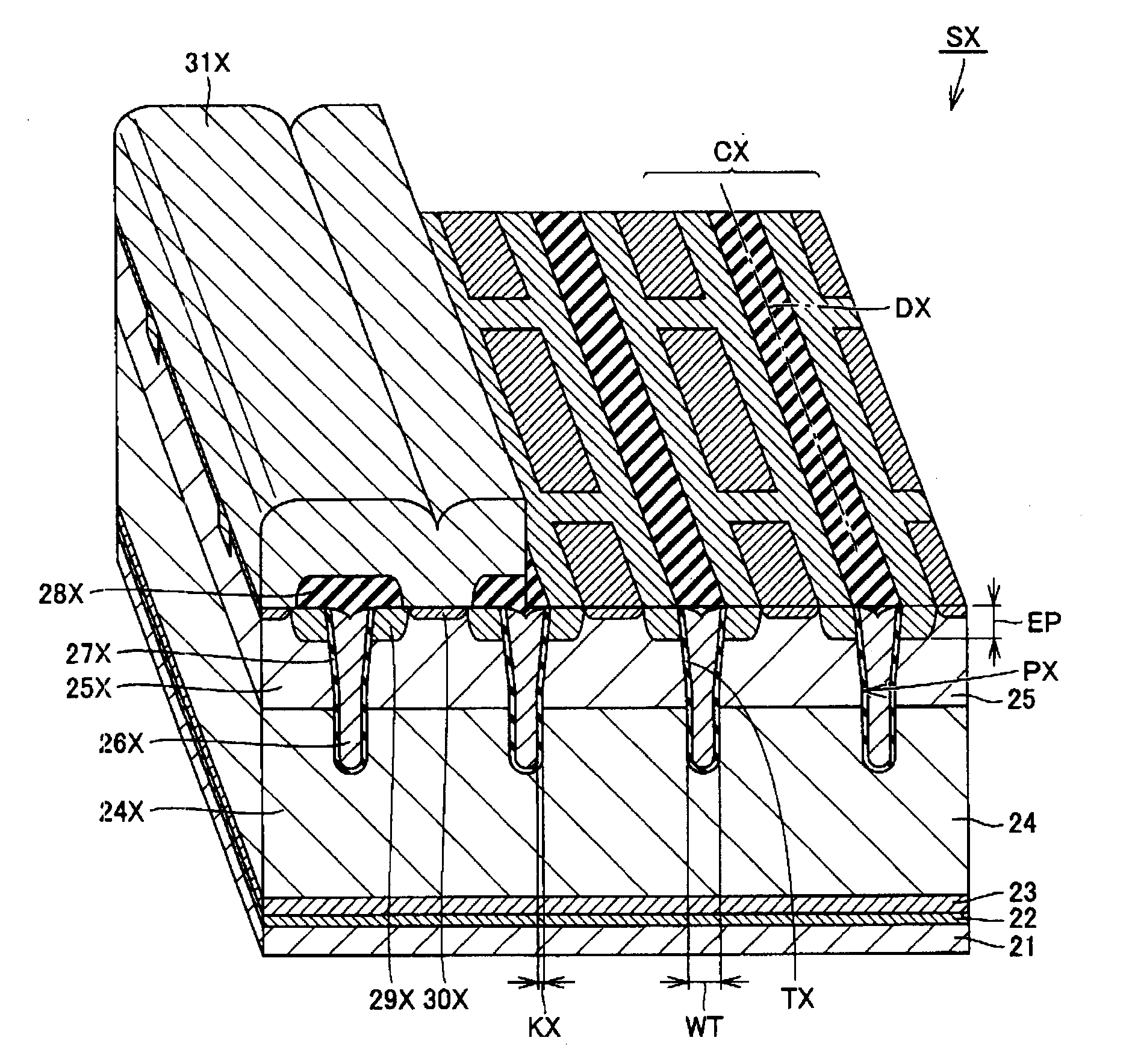
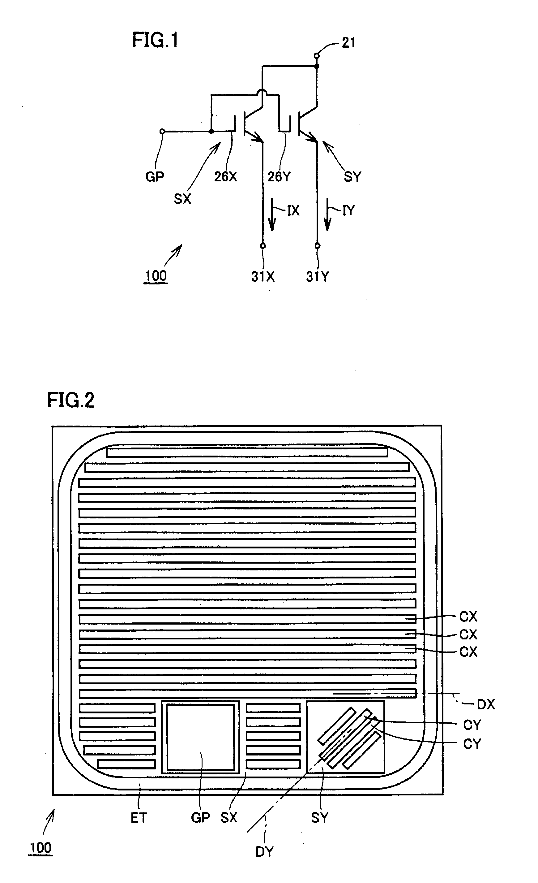
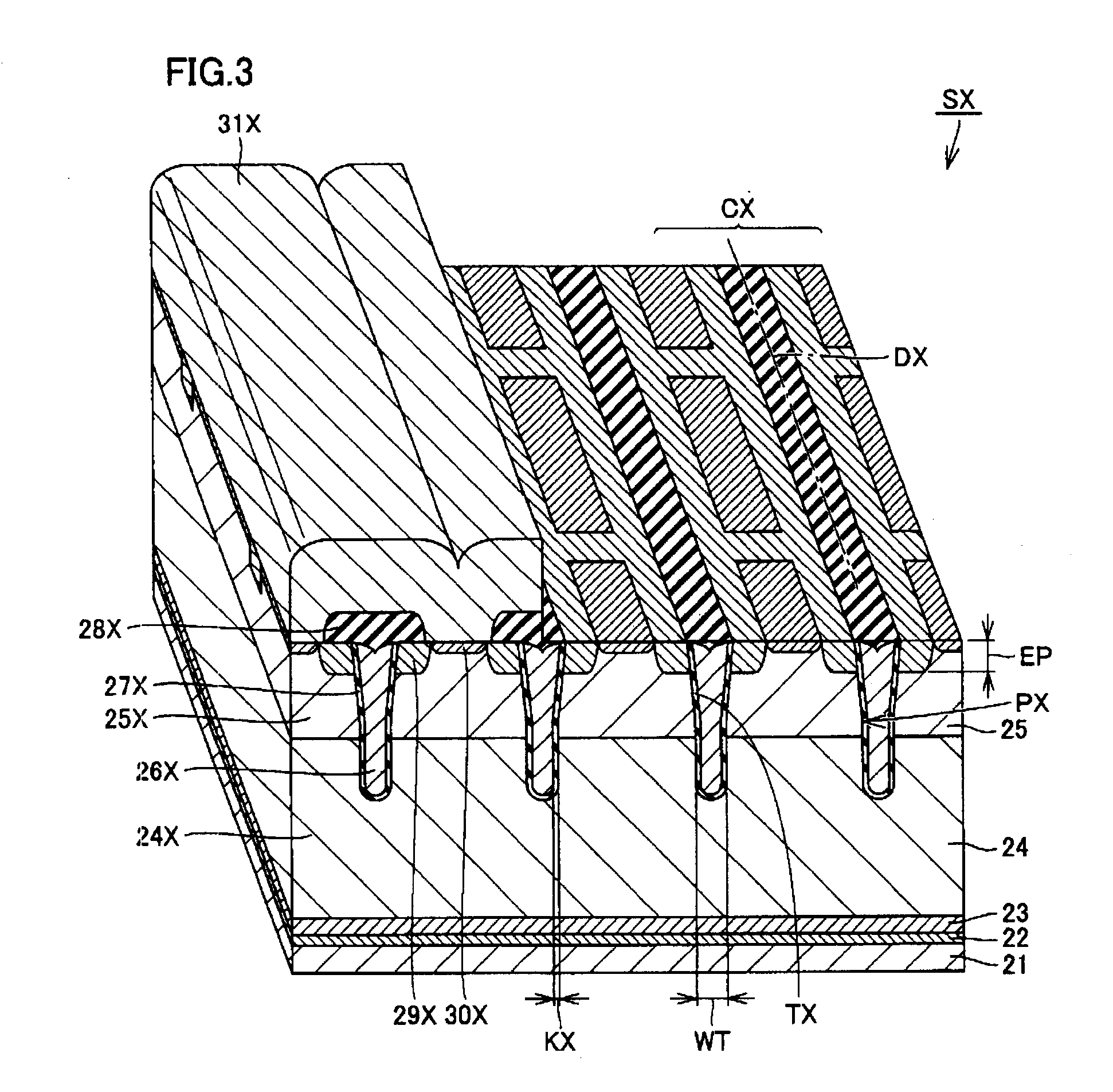
[0042]Referring to FIG. 1, a semiconductor device 100 in the present embodiment is a power semiconductor device, and includes a main portion SX (first semiconductor element portion), a sense portion SY (second semiconductor element portion), and a gate pad GP. Main portion SX and sense portion SY are IGBT portions for switching a main current IX (first current) and a sense current IY (second current), respectively, in accordance with a voltage of gate pad GP. An absolute value of sense current IY is smaller than an absolute value of main current IX, e.g., about one-thousandth of the absolute value of main current IX, and a waveform of sense current IY substantially corresponds to a waveform of main current IX. Thus, sense current IY can be used as a current for monitoring a value of main current IX in order to check whether it is excessive or not.

[0043]Main portion SX includes a main gate electrode 26X as its gate electrode, a main emitter electrode 31X as its emitter electrode, and...

second embodiment

[0083]Referring mainly to FIG. 7, a semiconductor device according to the present embodiment includes a sense portion SYa instead of sense portion SY (FIG. 4) in the first embodiment. Sense portion SYa includes a sense cell CYa arranged similarly to sense cell CY (FIG. 4).

[0084]Sense portion SYa also includes, instead of sense n+ source portion 29Y of sense portion SY (FIG. 4), a sense n+ source portion 29Ya having a depth EPa different from depth EP of sense n+ source portion 29Y for each sense cell CYa. With this configuration, depth EP (FIG. 3) of main n+ source portion 29X (first source portion) of main portion SX and depth EPa (FIG. 7) of sense n+ source portion 29Ya (second source portion) of sense portion SYa in the semiconductor device according to the present embodiment are different from each other.

[0085]The configuration is otherwise substantially the same as in the first embodiment described above, and thus the same or corresponding elements have the same characters and ...

third embodiment

[0097]A semiconductor device according to the present embodiment includes a main portion SXb (FIG. 11) and a sense portion SYb (FIG. 12) instead of main portion SX (FIG. 3) and sense portion SY (FIG. 4) in the first embodiment, respectively.

[0098]Referring to FIG. 11, main portion SXb includes a main cell CXb arranged similarly to main cell CX (FIG. 3). Main portion SXb also includes, instead of main n+ source portion 29X and main p+ contact portion 30X of main portion SX (FIG. 3), a main n+ source portion 29Xb and a main p+ contact portion 30Xb, respectively, for each main cell CXb. Main n+ source portion 29Xb and main p+ contact portion 30Xb are arranged in stripes along main direction DX when viewed two-dimensionally, and constitutes a so-called stripe structure. Main n+ source portion 29Xb and main p+ contact portion 30Xb have a first source width WnX and a first contact width WpX (first width) along main direction DX, respectively. Thus, the plurality of main n+ source portions...


PUM


Abstract

A first semiconductor element portion for switching a first current includes a first channel surface having a first plane orientation. A first region of a semiconductor layer includes a first trench having the first channel surface. A first gate insulating film covers the first channel surface with a first thickness. A second semiconductor element portion for switching a second current smaller than the first current includes a second channel surface having a second plane orientation different from the first plane orientation. A second region of the semiconductor layer includes a second trench having the second channel surface. A second gate insulating film covers the second channel surface with a second thickness larger than the first thickness.

Description

BACKGROUND OF THE INVENTION[0001]1. Field of the Invention[0002]The present invention relates to a semiconductor device and a method of manufacturing the same, and more particularly to a semiconductor device having a gate electrode formed to fill a trench and a method of manufacturing the same.[0003]2. Description of the Background Art[0004]There are semiconductor devices including a main electrode for supplying a current to be switched, i.e., a main current, to a semiconductor layer, and a gate electrode for applying an electric field to the semiconductor layer, and performing switching by controlling a channel of the semiconductor layer with the electric field generated by the gate electrode. A MOS (Metal Oxide Semiconductor) transistor or an IGBT (Insulated Gate Bipolar Transistor) are representative examples of such semiconductor devices. Particularly in power control applications, a structure in which a number of cells each capable of performing switching operation are connecte...

Claims


Application Information

Patent Timeline
IPC IPC(8): H01L27/088H01L21/336
CPCH01L21/823487H01L27/088H01L29/045H01L29/0696H01L29/0834H01L29/42368H01L29/4238H01L2924/0002H01L29/66348H01L29/7397H01L29/7813H01L29/7815H01L2924/00H01L29/7811
Inventor TAKANO, KAZUTOYO
Owner MITSUBISHI ELECTRIC CORP
Why Eureka
Try Eureka