Method for fabricating phase change memory device
a memory device and phase change technology, applied in the direction of semiconductor devices, basic electric elements, electrical equipment, etc., can solve the problems of increasing the current to be carried through the heater electrode, reducing the heat transfer efficiency of the heater electrode to the phase change layer, etc., to achieve the effect of reducing the amount of energy consumed by the heater electrode during phase changes and reducing the power consumption of the phase change memory devi
- Summary
- Abstract
- Description
- Claims
- Application Information
AI Technical Summary
Benefits of technology
Problems solved by technology
Method used
Image

Examples
first embodiment
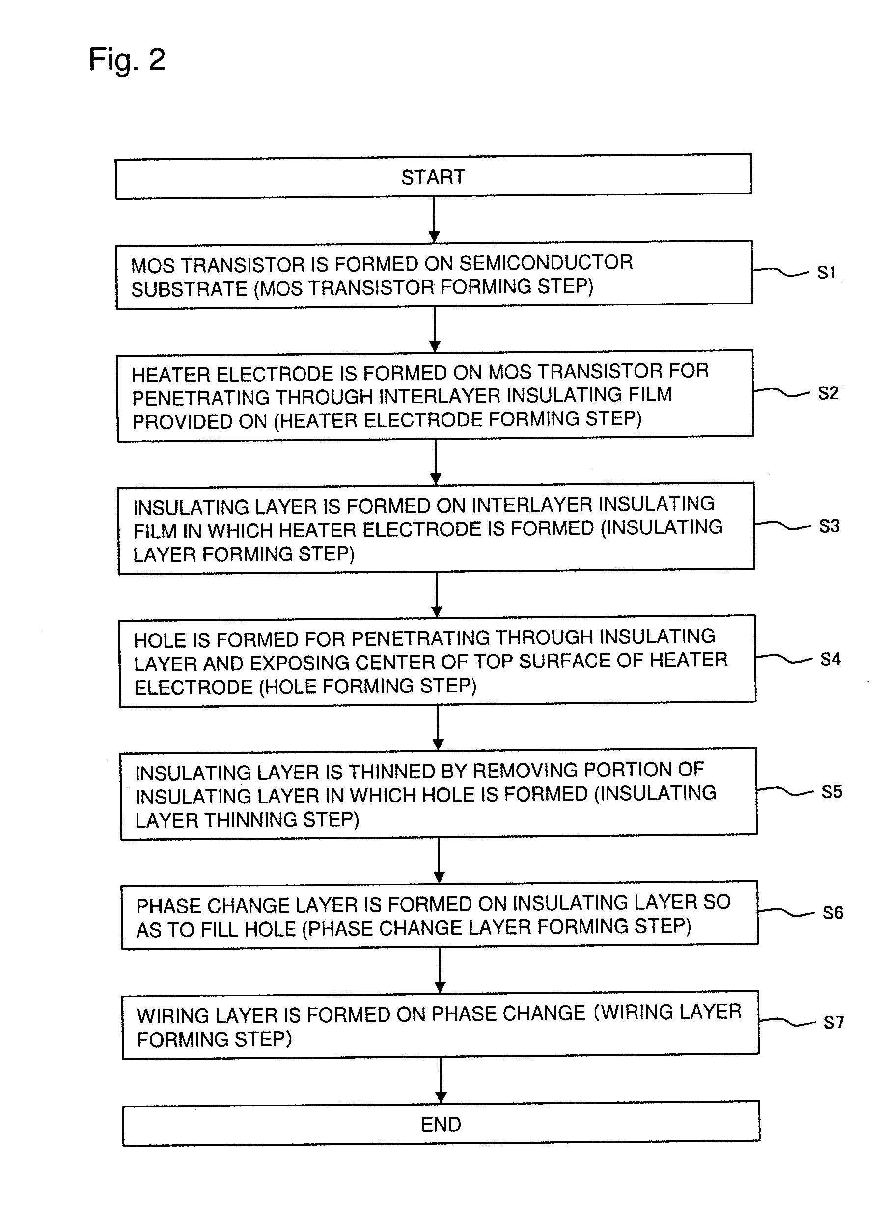
[0020]First, a method for fabricating a PRAM as a phase change memory device in the present invention will be described with reference to FIGS. 1 to 10.
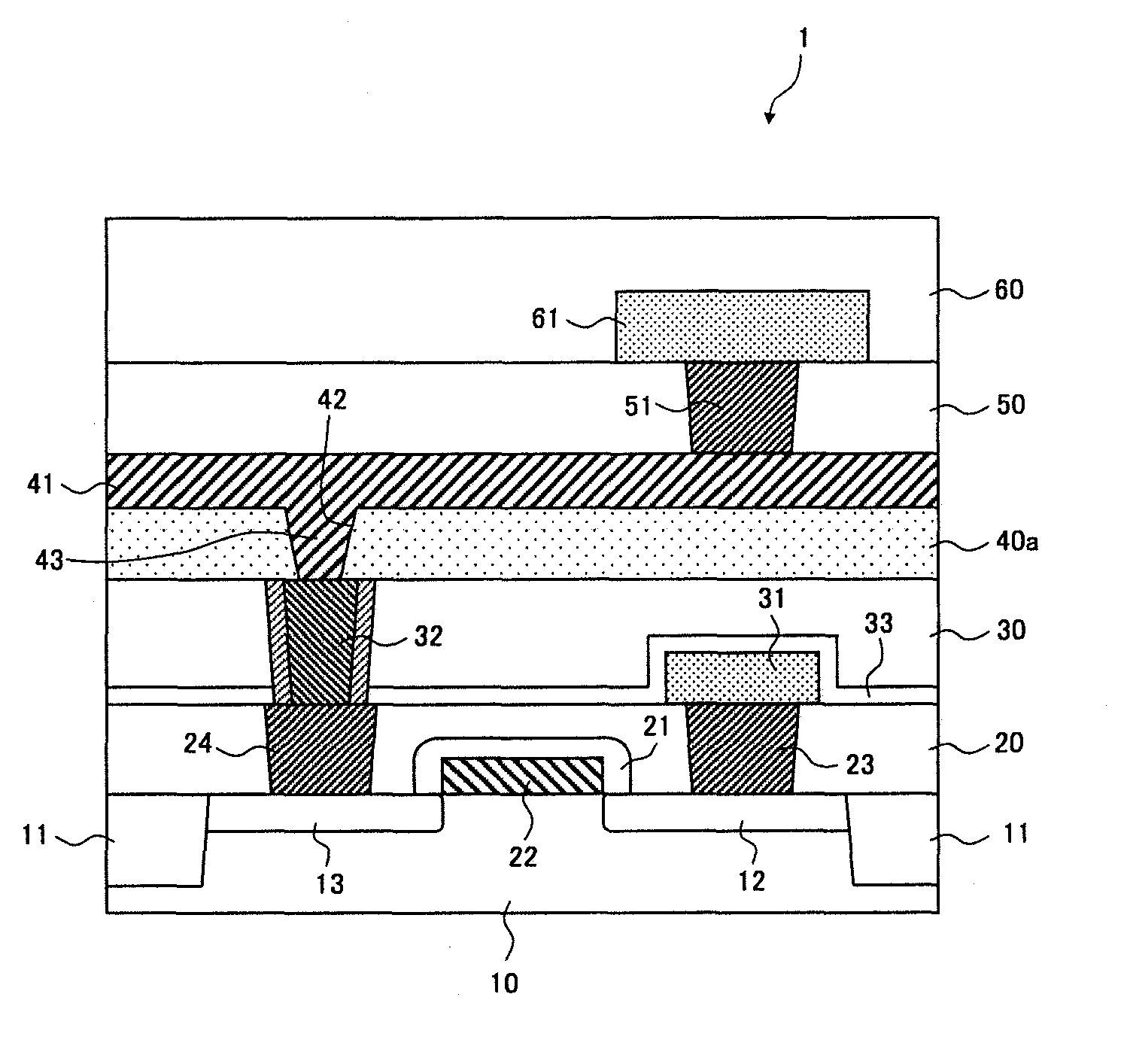
[0021]FIG. 1 is a cross sectional view of the PRAM to be produced by the fabricating method of this embodiment, showing a cross section of a memory cell region, in which a MOS transistor is formed, taken along a direction perpendicular to a semiconductor substrate.
[0022]PRAM 1 of this embodiment includes a MOS transistor as a switching device and phase change layer 41 as a memory element.
[0023]The MOS transistor is formed in an area surrounded by isolation region 11 on semiconductor substrate 10 made of silicon, the MOS transistor comprising diffusion regions 12, 13 and gate electrode 22 whose surface is covered with insulating film 21. One diffusion region 12 of the MOS transistor is connected to wiring 31 through contact plug 23 provided in interlayer insulating film 20, and other diffusion region 13 is connected to heater electrod...
second embodiment
[0059]FIGS. 11 to 13 are diagrams showing steps from the insulating layer forming step (Step S3) to the insulating layer thinning step (Step S5) in a
[0060]As described above, in the insulating layer forming step of the embodiment shown in FIGS. 5 to 7, insulating layer 40 having a two-layer structure consisting of upper insulating film 40b and lower insulating film 40a was formed on heater electrode 32. On the other hand, in this embodiment, as shown in FIG. 11, single-layered insulating layer 40c made of a silicon oxide film having a thickness of 115 nm is formed on heater electrode 32 by low-pressure CVD.
[0061]In this case, in the hole forming step shown in FIG. 12, hole 42 is formed for penetrating through insulating layer 40c and exposing heater electrode 32 therebelow. Thereafter, in the insulating layer thinning step, as shown in FIG. 13, a portion of insulating layer 40c is removed by wet etching in order to reduce the thickness of insulating layer 40c. The processing time fo...
PUM
 Abstract
Description
Claims
Application Information
 - Generate Ideas
- Intellectual Property
- Life Sciences
- Materials
- Tech Scout
- Unparalleled Data Quality
- Higher Quality Content
- 60% Fewer Hallucinations
Browse by: Latest US Patents, China's latest patents, Technical Efficacy Thesaurus, Application Domain, Technology Topic, Popular Technical Reports.
© 2025 PatSnap. All rights reserved.Legal|Privacy policy|Modern Slavery Act Transparency Statement|Sitemap|About US| Contact US: help@patsnap.com