Non-volatile semiconductor storage device
a semiconductor storage device and non-volatile technology, applied in digital storage, redundant hardware error correction, instruments, etc., can solve the problems of difficult to improve reading speed, reduce the likelihood of erroneous reading, and may occur erroneous reads
- Summary
- Abstract
- Description
- Claims
- Application Information
AI Technical Summary
Problems solved by technology
Method used
Image


Examples
first embodiment
Configuration of Semiconductor Storage Device in First Embodiment
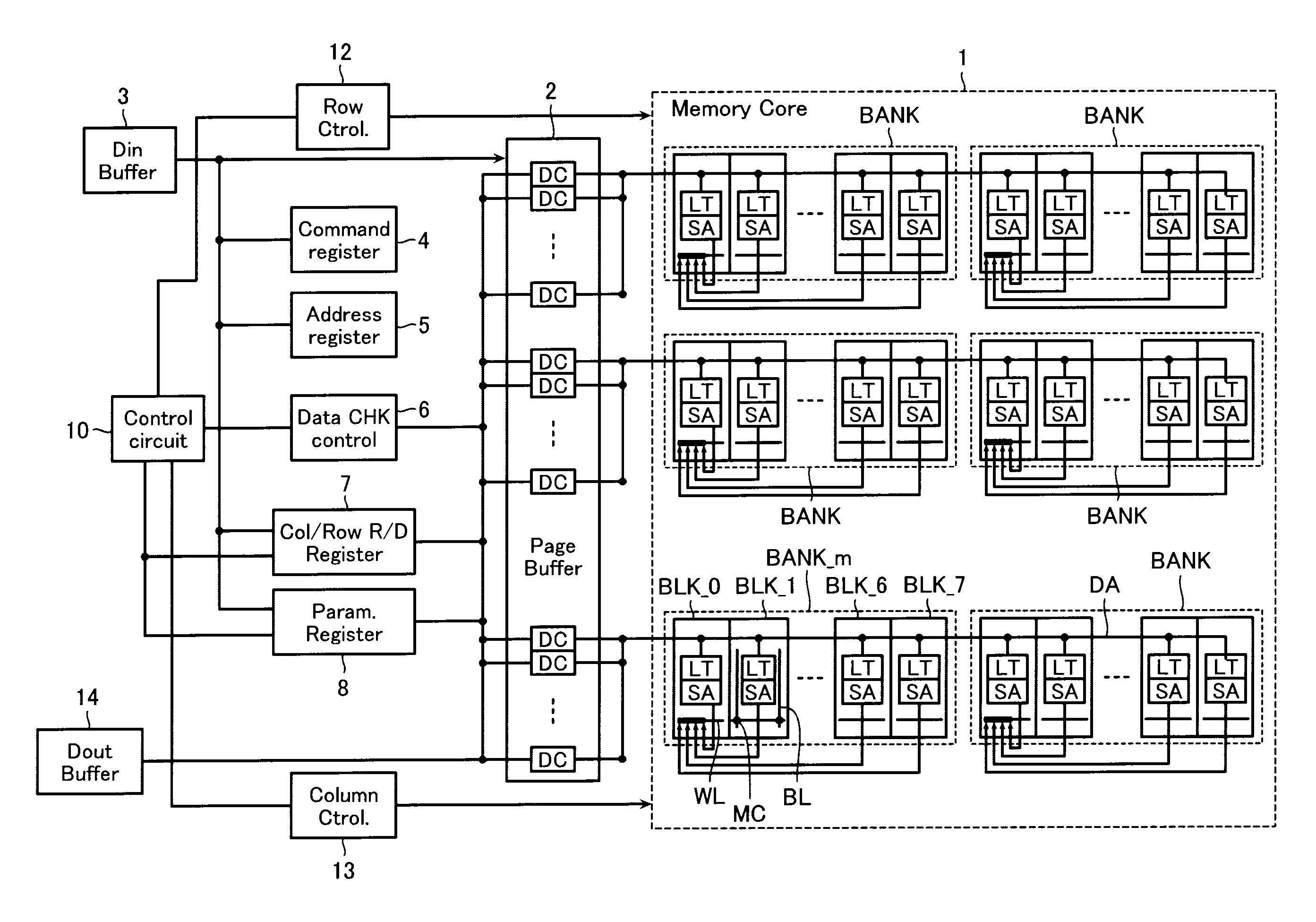
[0029]FIG. 1 is a block diagram illustrating an example of the entire configuration of a semiconductor storage device according to a first embodiment. FIG. 2 illustrates an example of a part of the layout of one memory block BLK in FIG. 1.
[0030]The semiconductor storage device according to the first embodiment comprises a memory core 1 including a plurality of memory cells MC. The memory core 1 includes a plurality of (e.g., 32) memory banks BANK arranged therein. Each memory bank BANK includes a plurality of (e.g., 8) memory blocks BLK. A plurality of (e.g., 2048) bit lines BL and a plurality of (e.g., 512) word lines WL are arranged to intersect each other in each memory block BLK. Memory cells MC are arranged at respective intersections between the bit lines and the word lines. The memory cells MC are resistive memory elements as described below.
[0031]As illustrated in FIG. 1, each memory bank BANK is provided with ...
second embodiment
[0068]Referring now to FIGS. 6 to 8, the non-volatile semiconductor storage device according to a second embodiment will be described below. The device configuration is similar to that of the first embodiment (FIGS. 1 and 2), and description thereof will be omitted. The procedure for reading normal data is also substantially the same as that described in the first embodiment. This embodiment is different from the first embodiment in the way of reading initial setting data (ROM fuse data).
[0069]FIG. 6 is a conceptual diagram describing a procedure for reading ROM fuse data according to this embodiment. When ROM fuse data (a to h) of one column is read through the input / output data lines I / O0 to I / O7, the controller 10 performs a read operation corresponding to the second read operation of FIG. 4 from the beginning of the read operation, without performing a read operation corresponding to the first read operation of FIG. 4 (Read1 of FIG. 4). That is, as illustrated in FIG. 6, a read ...
third embodiment
[0073]Referring now to FIGS. 9 to 11, the non-volatile semiconductor storage device according to a third embodiment will be described below. The device configuration is similar to that of the first embodiment (FIGS. 1 and 2), and description thereof will be omitted. The procedure for reading normal data is also substantially the same as that described in the first embodiment. This embodiment is different from the second embodiment in the form of storing initial setting data (ROM fuse data) and in the way of reading ROM fuse data.
[0074]In this embodiment, not only ROM fuse data Data1 (a to h), but also the complementary data Data2 ( / a to / h) are stored as illustrated in FIG. 9. Then, the data Data1 and Data2 are read concurrently. Furthermore, an exclusive OR operation between these data is performed at the data check control circuit 6 to determine whether the ROM fuse data is correct or incorrect. As is the case with the second embodiment (FIG. 6), ROM fuse data of one column is als...
PUM
 Abstract
Description
Claims
Application Information
 - R&D
- Intellectual Property
- Life Sciences
- Materials
- Tech Scout
- Unparalleled Data Quality
- Higher Quality Content
- 60% Fewer Hallucinations
Browse by: Latest US Patents, China's latest patents, Technical Efficacy Thesaurus, Application Domain, Technology Topic, Popular Technical Reports.
© 2025 PatSnap. All rights reserved.Legal|Privacy policy|Modern Slavery Act Transparency Statement|Sitemap|About US| Contact US: help@patsnap.com