Group III nitride semiconductor device, production method therefor, power converter

a semiconductor device and nitride technology, applied in semiconductor devices, semiconductor/solid-state device details, electrical apparatus, etc., can solve the problems of reduced mobility of 2deg generated at the heterojunction interface between the carrier transport layer and the carrier supply layer, increase in on-state resistance, and safety problems, so as to improve the breakdown voltage and low loss , the effect of high performan

Active Publication Date: 2011-03-24
TOYODA GOSEI CO LTD
View PDF5 Cites 81 Cited by
  • Summary
  • Abstract
  • Description
  • Claims
  • Application Information

AI Technical Summary

Benefits of technology

[0008]In view of the foregoing, an object of the present invention is to provide a Group III nitride semiconductor device with reduced on-state resistance. Another object of the present invention is to provide a method for producing the semiconductor device. Yet another object of the present invention is to provide a power converter comprising the semiconductor device.

Problems solved by technology

However, an HEMT exhibiting a normally-on characteristic poses a safety problem.
However, when the structure disclosed in Japanese Patent Application Laid-Open (kokai) No. 2008-147593 is produced through the method using selective re-growth disclosed in Japanese Patent Application Laid-Open (kokai) No. 2009-99691, problems arise in that, for example, impurities, etc. are incorporated at the interface between a carrier transport layer and a carrier supply layer when the carrier supply layer is grown on the carrier transport layer, and flatness of the interface between these layers is degraded, which results in reduction in mobility of 2DEG generated at the heterojunction interface between the carrier transport layer and the carrier supply layer, and an increase in on-state resistance.

Method used


Image

  • Group III nitride semiconductor device, production method therefor, power converter
  • Group III nitride semiconductor device, production method therefor, power converter
  • Group III nitride semiconductor device, production method therefor, power converter

Examples


embodiment 1

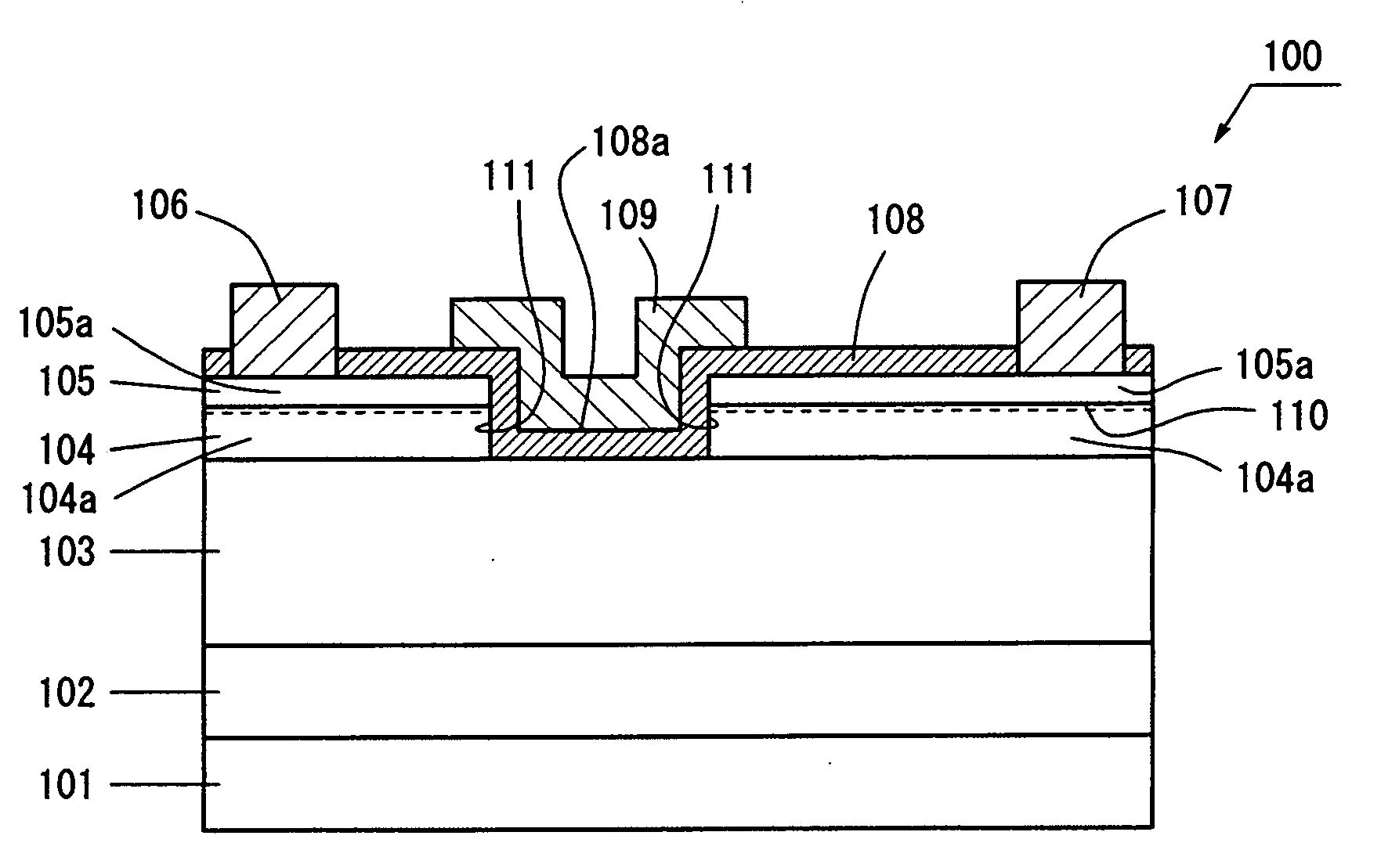
[0077]FIG. 1 shows the configuration of an HEMT 100 according to Embodiment 1.

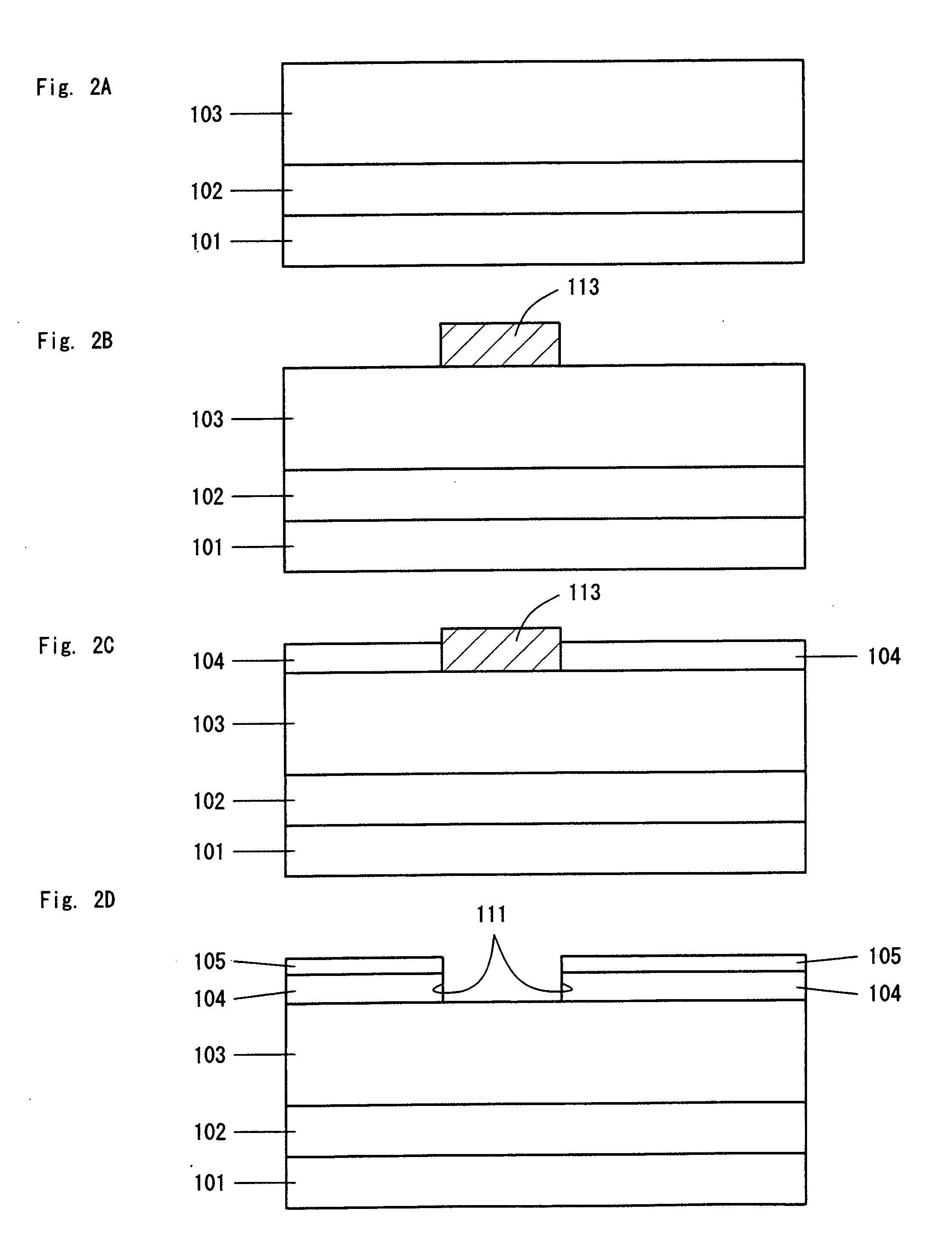
[0078]The HEMT 100 includes an Si substrate 101; an AlN buffer layer 102 provided on the substrate 101; and a first carrier transport layer 103 formed of undoped GaN and provided on the AlN buffer layer 102.

[0079]Two separate second carrier transport layers 104 formed of undoped GaN are provided on two separate regions of the first carrier transport layer 103. Carrier supply layers 105 formed of Al0.25Ga0.75N are respectively provided on the two separate second carrier transport layers 104. The second carrier transport layer 104 and the carrier supply layer 105 form a heterojunction therebetween. The heterojunction forms a channel on which electrons conduct. The second carrier transport layer 104 and the carrier supply layer 105 are respectively formed through selective crystal re-growth.

[0080]A source electrode 106 is formed on one of the two separate carrier supply layers 105, and a drain electrode 107 i...

embodiment 2

[0105]FIG. 3 shows the configuration of an HEMT 200 according to Embodiment 2. The HEMT 200 has the same configuration as the HEMT 100 according to Embodiment 1, except that the second carrier transport layer 104, the carrier supply layer 105, the insulating film 108, and the gate electrode 109 are respectively replaced with a second carrier transport layer 204, a carrier supply layer 205, an insulating film 208, and a gate electrode 209. The second carrier transport layer 204 and the carrier supply layer 205 differ from the second carrier transport layer 104 and the carrier supply layer 105 only in that two mutually facing lateral end surfaces 220 of two separate laminate structures each including the second carrier transport layer 204 and the carrier supply layer 205 are inclined. Similar to the case of the second carrier transport layer 104 and the carrier supply layer 105, the second carrier transport layer 204 and the carrier supply layer 205 are formed through selective re-gro...

embodiment 3

[0108]FIG. 4 shows the configuration of an HEMT 300 according to Embodiment 3. The HEMT 300 has the same configuration as the HEMT 100 according to Embodiment 1, except that the carrier supply layer 105 is replaced with a carrier supply layer 305 as described below. The carrier supply layer 305 has a three-layer structure including a first carrier supply layer 305a formed of undoped GaN, a second carrier supply layer 305b formed of undoped AlGaN, and a third carrier supply layer 305c formed of undoped AlN, which layers are sequentially stacked on the second carrier transport layer 104. The second carrier transport layer 104 is selectively re-grown on the first carrier transport layer 103 and the carrier supply layer 305 is selectively grown on the second carrier transport layer 104 similar to the case of the second carrier transport layer 104 and the carrier supply layer 105 in Embodiment 1, respectively.

[0109]In the HEMT 300, the second carrier transport layer 104 and the carrier s...


PUM


Abstract

Provided is an HEMT exhibiting a normally-off characteristic and low on-state resistance, which includes a first carrier transport layer; two separate second carrier transport layers formed of undoped GaN and provided on two separate regions of the first carrier transport layer; and carrier supply layers formed of AlGaN and respectively provided on the two separate second carrier transport layers. The second carrier transport layers and the carrier supply layers are respectively formed through crystal growth on the first carrier transport layer. The heterojunction interface between the second carrier transport layer and the carrier supply layer exhibits high flatness, and virtually no growth-associated impurities are incorporated in the vicinity of the heterojunction interface. Therefore, reduction in mobility of 2DEG is prevented, and on-state resistance is reduced.

Description

BACKGROUND OF THE INVENTION[0001]1. Field of the Invention[0002]The present invention relates to a Group III nitride semiconductor device, and to a method for producing the device. More particularly, the present invention relates to a semiconductor device with reduced on-state resistance (e.g., an HEMT (high electron mobility transistor), also called an HFET (heterostructure field effect transistor), the term of HEMT is used in the present specification, or a diode), and to a method for producing the device. The present invention also relates to a power converter including such a Group III nitride semiconductor device.[0003]2. Background Art[0004]Group III nitride semiconductors have been widely used as a material for light-emitting devices. Also, Group III nitride semiconductors are envisaged as a material for power devices, since they exhibit high electron mobility and have a breakdown field strength about 10 times that of Si. Hitherto developed power devices include an HEMT (high...

Claims


Application Information

Patent Timeline
Patent Type & Authority Applications(United States)
IPC IPC(8): H01L29/737H01L21/20
CPCH01L23/291H01L23/3171H01L29/2003H01L29/407H01L29/4236H01L29/66462H01L2924/0002H01L29/7785H01L29/7787H01L29/861H01L2924/00
Inventor OKA, TORU
Owner TOYODA GOSEI CO LTD
Why Eureka
Try Eureka