

Method and apparatus for uniform microwave treatment of semiconductor wafers
a technology of uniform heating and semiconductor wafers, applied in the direction of optical radiation measurement, muffle furnaces, furnaces, etc., can solve the problems of inability to use fixed-frequency microwaves for this application, the entire wafer is contaminated, and the use of fixed-frequency microwaves is generally unsuccessful, so as to improve the temperature control and heat large semiconductor wafers uniformly
- Summary
- Abstract
- Description
- Claims
- Application Information
AI Technical Summary
Benefits of technology
Problems solved by technology
Method used
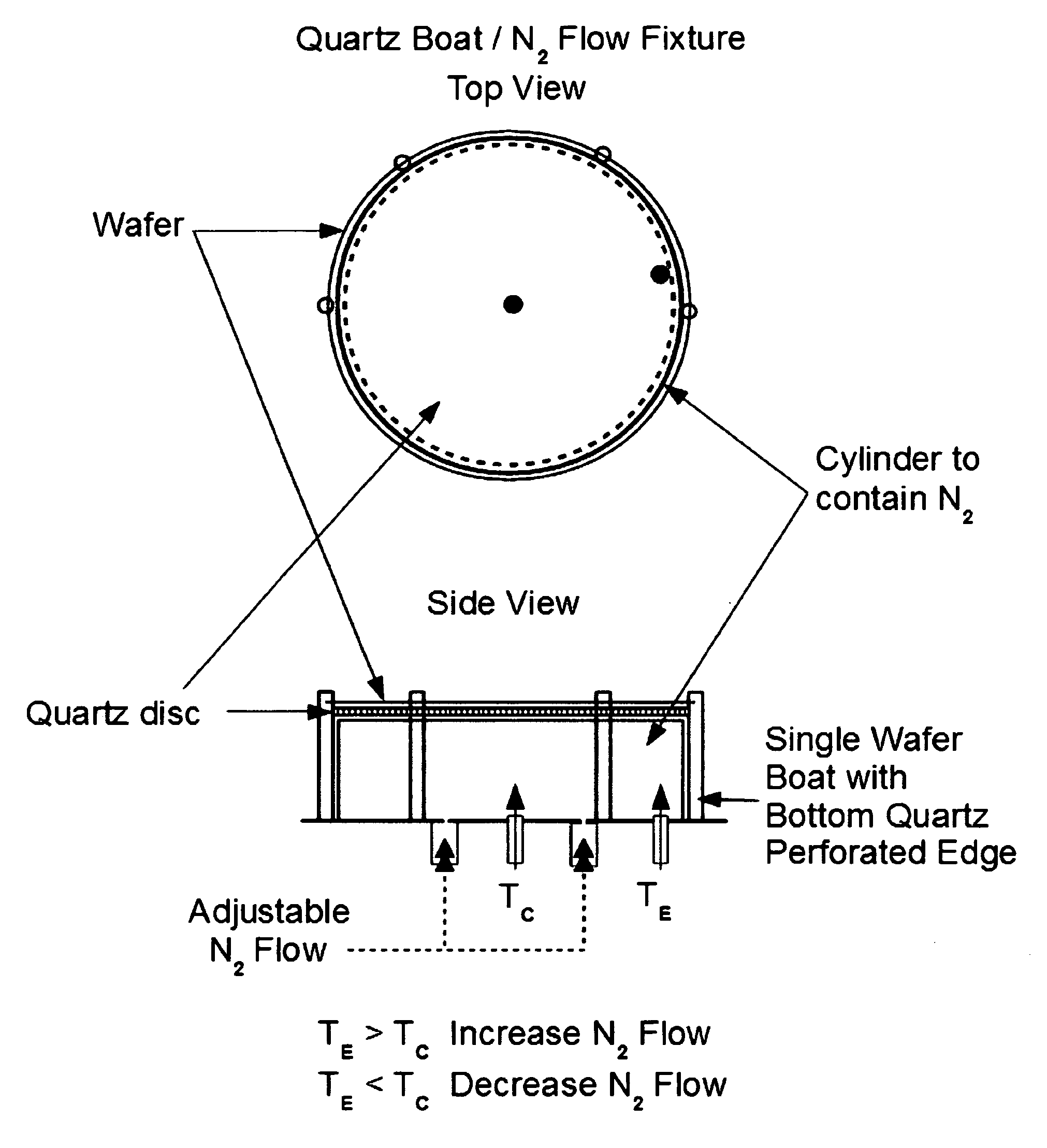
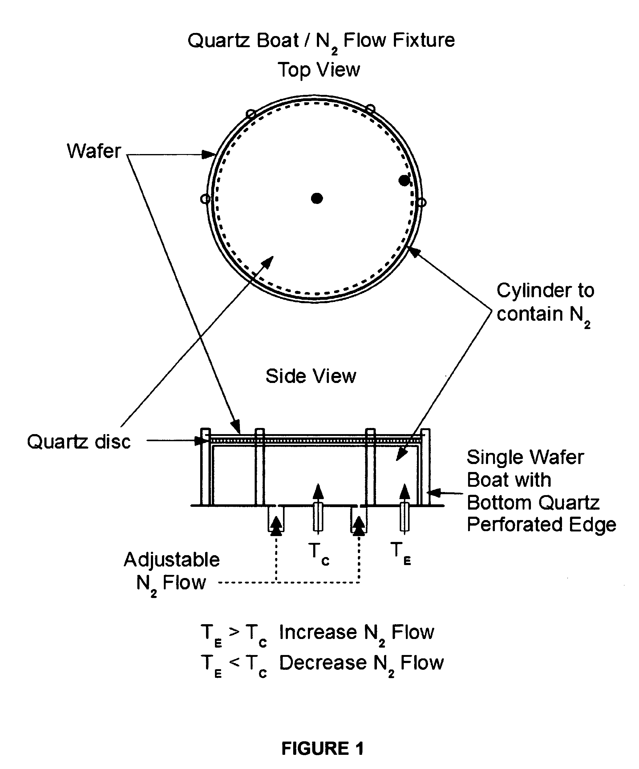
Image

Examples
example
[0069]Flat panel displays: The use and processing of ITO leads to another example, viz., Flat Panel Displays (FPD) that encompass a growing number of technologies enabling video displays that are much lighter and thinner than traditional television and video displays that use cathode ray tubes. FPD can be divided into two general categories:
1. Volatile displays require that the pixels be periodically refreshed to retain their state, even when displaying a static image. This refresh typically occurs many times a second. These include: Plasma displays; Liquid crystal displays (LCDs); Organic light-emitting diode displays (OLEDs); Light-emitting diode displays (LED); Electro-luminescent displays (ELDs); Surface-conduction electron-emitter displays (SEDs); and Field emission displays (FEDs), also called Nano-emissive displays (NEDs).
2. Static flat panel displays rely on materials where the color states are bistable. No energy is required to maintain the image instead energy is required ...
PUM
 Abstract
Description
Claims
Application Information