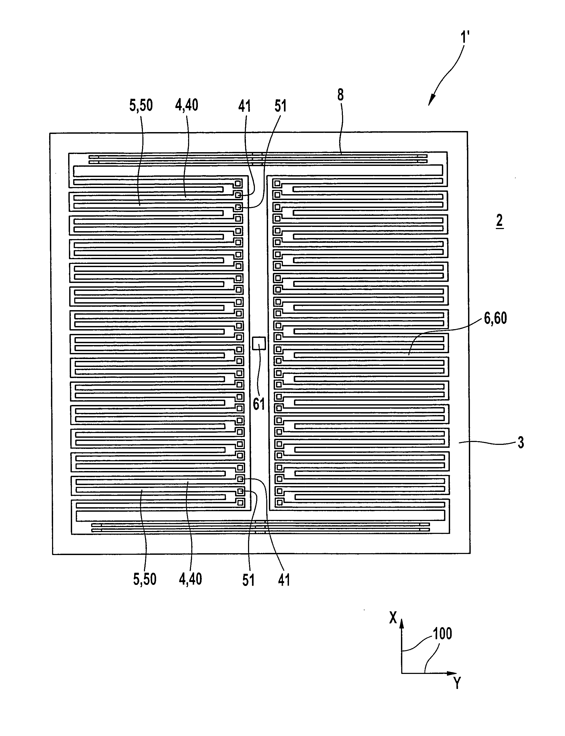
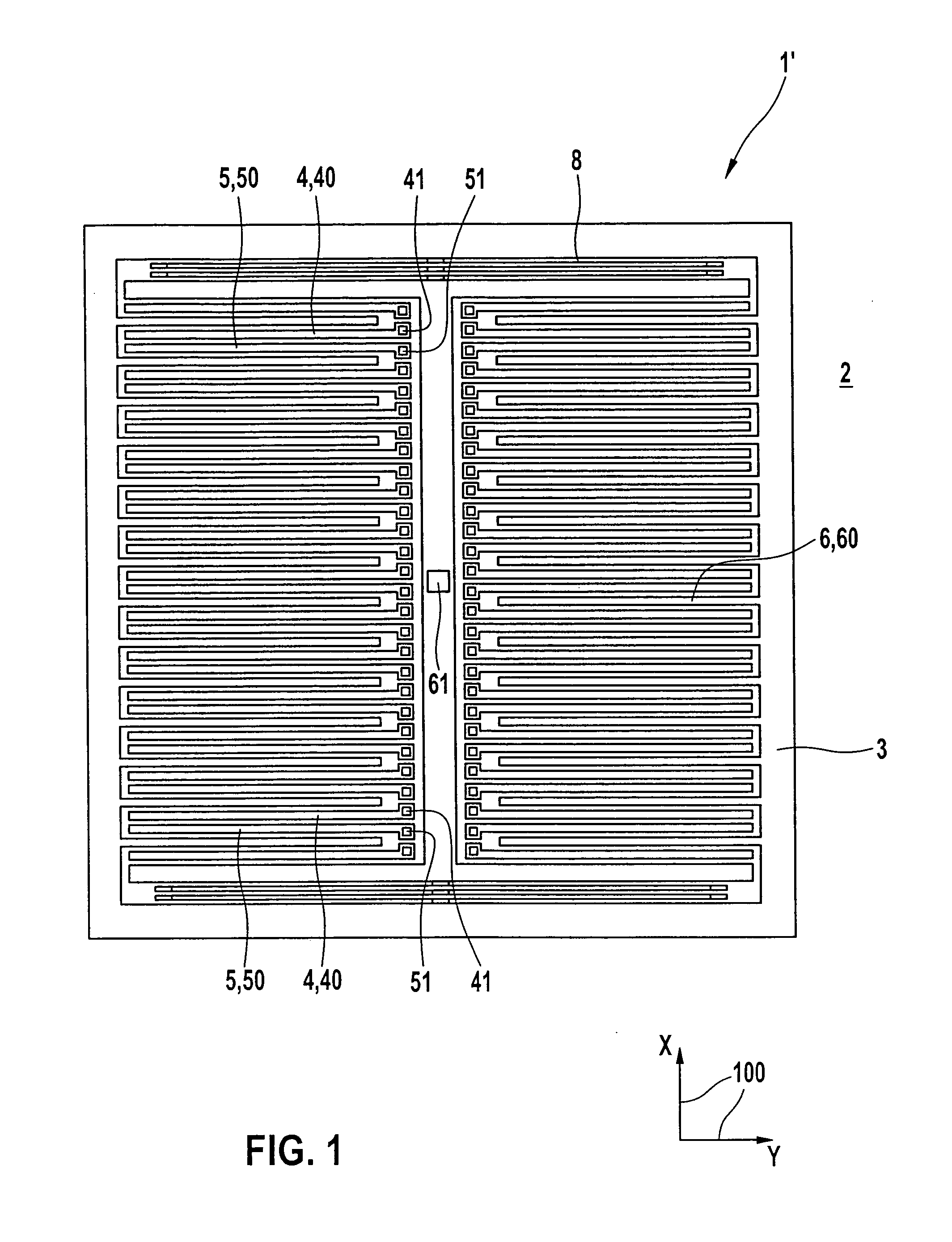
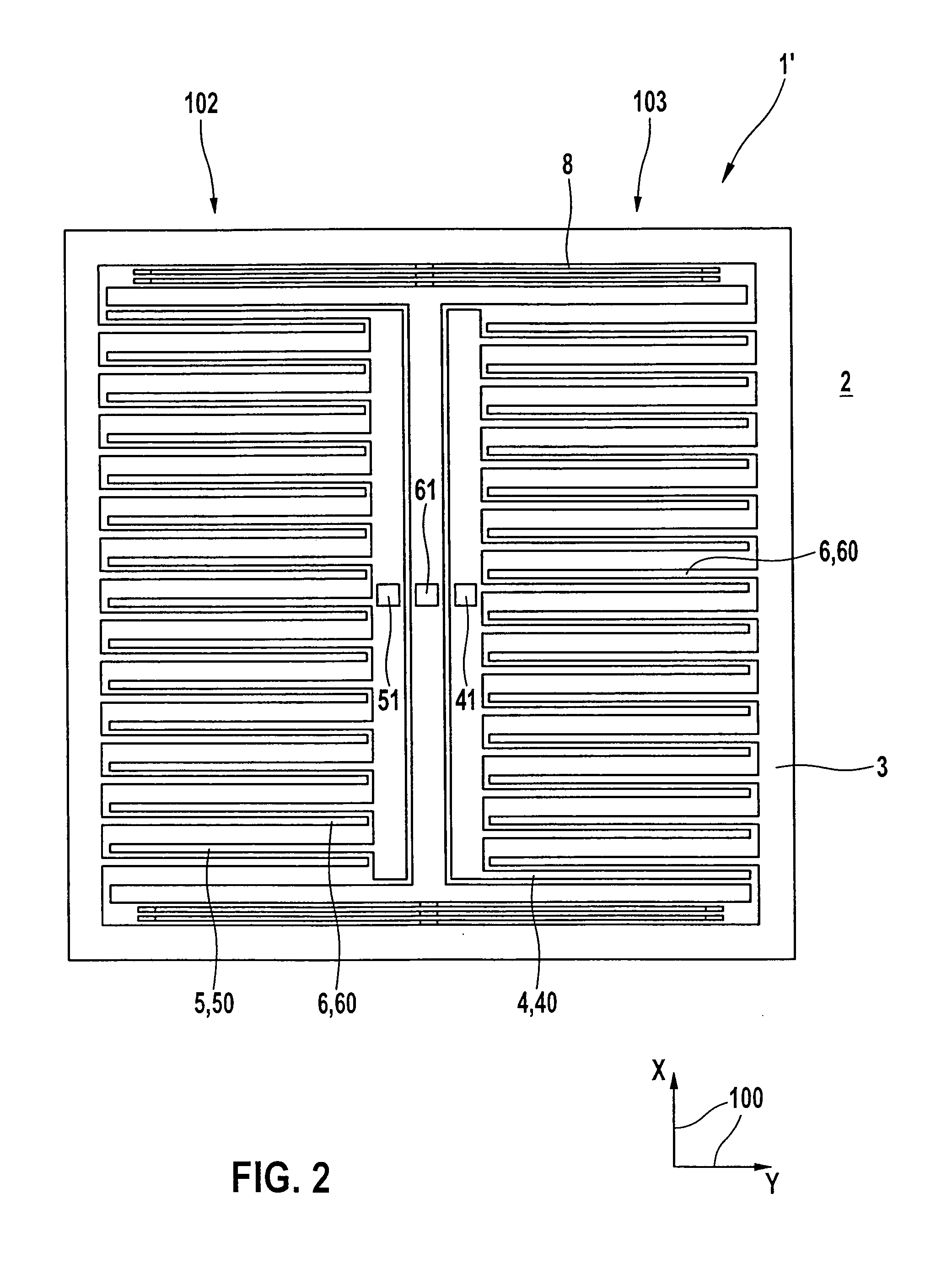
[0005]The micromechanical structure according to the present invention and the method according to the present invention for manufacturing a micromechanical structure provide the
advantage over the related art that, with the aid of the first and the second electrode structures, a fully differential evaluation of a deflection of the
seismic mass relative to the substrate may be achieved, and at the same time the first electrode structure as well as the second electrode structure are mounted on the substrate in a
central region of the micromechanical structure in order to decouple stress. As a result, on the one hand high sensitivity and a comparatively good
signal-to-
noise ratio may be achieved in the detection of the deflection, and on the other hand, stress on the first and second electrode structures may be effectively decoupled from the substrate, thus increasing the offset stability, i.e., zero point stability, of the micromechanical structure. In particular, relative movements between the counterelectrode structure and the first and second electrode structures due to substrate warping, which otherwise would result in offset shifts, are thus avoided. Such substrate warping occurs, for example, in mold packages subjected to stress over the temperature range or the service life, and are caused in particular by differing coefficients of
thermal expansion of the substrate material, the mold material, and / or an
adhesive material. The substrate preferably includes a
semiconductor substrate, and is particularly preferably a
silicon substrate. The central region of the micromechanical structure includes in particular the center of the micromechanical structure parallel to the main plane of extension, as well as the surroundings of the center parallel to the main plane of extension, the maximum extension of the central region parallel to the main plane of extension preferably being 60 percent, particularly preferably 40 percent, and very particularly preferably 30 percent, of the maximum extension of the micromechanical structure parallel to the main plane of extension along the first direction or along a second direction which is perpendicular to the first direction. The micromechanical structure preferably includes an acceleration sensor, and particularly preferably includes a lateral acceleration sensor having a sensing direction oriented parallel to the main plane of extension. The substrate preferably has printed conductors for electrically contacting the first and / or second electrode structure and / or the seismic
mass. The first anchoring element preferably includes a plurality of first anchoring elements situated in the central region, while the second anchoring element preferably includes a plurality of second anchoring elements situated in the central region.
[0006]According to one example embodiment, it is provided that the seismic
mass is coupled to a third anchoring region situated in the central region, the seismic
mass preferably being elastically coupled to the third anchoring region via spring elements. In this way, the seismic mass is advantageously attached in the central region of the micromechanical structure, thus greatly reducing the risk of relative movement between the counterelectrode structure on the one hand and the first and second electrode structures on the other hand solely as the result of substrate warping. In particular, the first, second, and / or third anchoring elements are essentially congruent with one another along a second direction which is perpendicular to the first direction and parallel to the main plane of extension, and / or are each centrally situated relative to the micromechanical structure along the first direction.
[0007]According to one example embodiment, it is provided that the first electrode structure has a first connection region situated at least partially between the second electrode structure and the substrate, and in particular between the
second finger electrodes and the substrate, perpendicular to the main plane of extension. The first connection region advantageously allows bridging of the second electrode structure, and thus a
crossover of two electrically separated regions which is cantilevered, i.e., decoupled from the substrate, i.e., in particular a
crossover of the first and second electrode structures, without the need for attaching the substrate to the first and second electrode structures. Such a
crossover makes it possible in particular to achieve fully differential evaluation; i.e., each of the
third finger electrodes is always situated between the first and
second finger electrodes, while at the same time it is possible to anchor the first and second electrode structures as well as the counterelectrode structure in the central region. In addition, this greatly simplifies the line routing within the micromechanical structure, so that the micromechanical structure is comparatively compact.

