Adaptive chuck for planar bonding between substrates

a planar bonding and adaptive chuck technology, applied in the direction of mechanical control devices, instruments, process and machine control, etc., can solve the problems of local warping and bending of substrates, and achieve the effect of reducing the bowing and warping of substrates for bonding

Inactive Publication Date: 2011-04-14
GLOBALFOUNDRIES INC
View PDF11 Cites 35 Cited by
  • Summary
  • Abstract
  • Description
  • Claims
  • Application Information

AI Technical Summary

Benefits of technology

[0008]In another embodiment of the present invention, an electrostatic chuck includes an array of sensor-conductor assemblies. Each sensor-conductor assembly includes a conductive chuck element, a sensor configured to detect a substrate upon contact, and a motor that moves the sensor and the conductive chuck element vertically. The sensor detects the degree of deviation of the non-planar surface of a substrate from a planar surface. The conductive chuck element attached to each sensor-motor assembly is electri

Problems solved by technology

Substrates are subject to local warping and bending due to internal stress.
In general, the combination of global bowing and local warping in each semiconductor substrate generates gaps in bonded structures employed to form stacked chips.
Presence of such a gap in

Method used


Image

  • Adaptive chuck for planar bonding between substrates
  • Adaptive chuck for planar bonding between substrates
  • Adaptive chuck for planar bonding between substrates

Examples


first embodiment

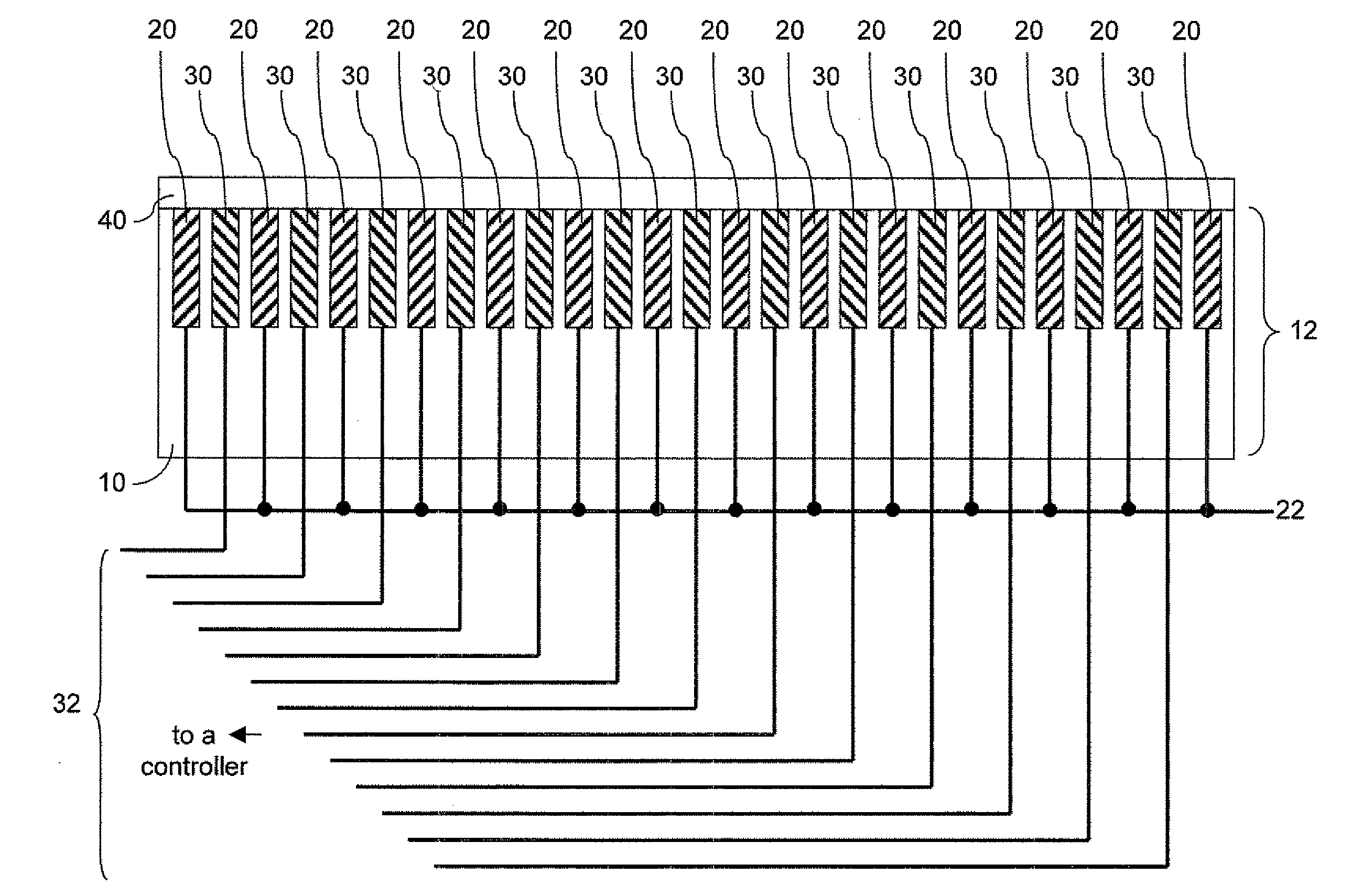
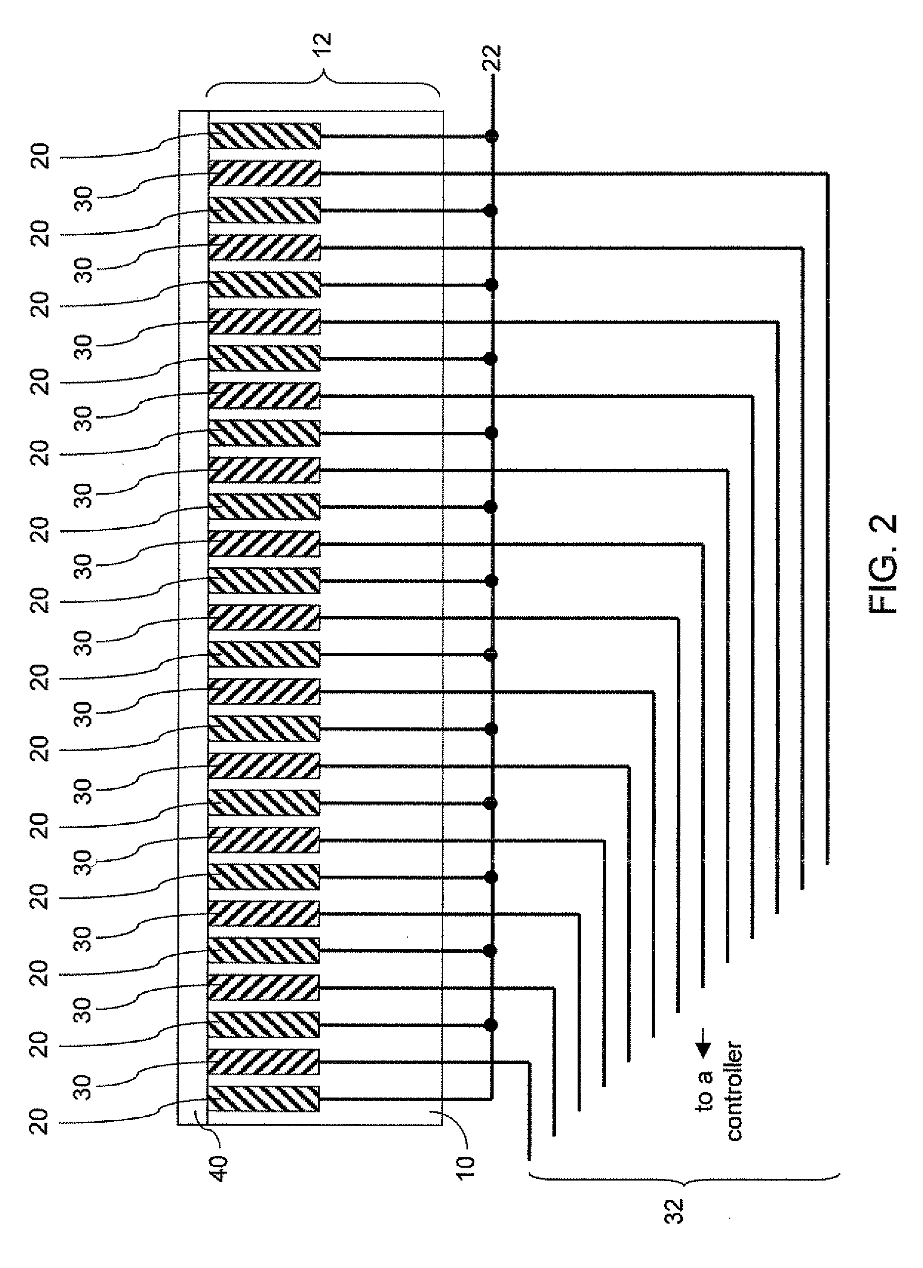
[0026]Referring to FIGS. 2 and 3, a first exemplary apparatus according to the present invention is shown. FIG. 2 is a vertical cross-sectional view of the first exemplary apparatus with a substrate 40 on a top surface thereof. FIG. 3 is a top-down view of the first exemplary apparatus without a substrate thereupon. In FIG. 2, the substrate 40 is shown as flattened, i.e., after bowing and warping of the substrate 40 is reduced to make a bottom surface of the substrate 40 more closely approximate the planar two-dimensional top surface of an insulating chuck body 10 through electrostatic biasing described below.

[0027]The first exemplary apparatus includes an electrostatic chuck 12 and a plurality of electrical lead wires 32 that are attached to the electrostatic chuck 12 to generate a locally non-uniform electrostatic potential field. The electrostatic chuck 12 includes the insulating chuck body 10 and an array of independently biased conductive chuck elements 30 embedded in the insul...

second embodiment

[0042]Referring to FIG. 6, a third exemplary structure according to the present invention includes an electrostatic chuck 14 and a plurality of electrical lead wires 32 that are attached to the electrostatic chuck 14 to generate a locally non-uniform electrostatic potential field. The electrostatic chuck 14 includes the insulating chuck body 10 and an array of sensor-conductor assemblies 39 embedded in the insulating chuck body 10. The insulating chuck body 10 has a planar top surface on which a substrate 40 can be placed. The substrate 40 is shown as provided, i.e., has the features of bending and warping inherently present in the substrate 40. The vertical scale is exaggerated compared with the horizontal scale for the substrate 40.

[0043]The sensor-conductor assemblies 39 in the array are electrically insulated from one another. Each of the sensor-conductor assemblies 39 includes an independently biased conductive chuck element 30, a sensor 34 configured to detect the substrate 40...

third embodiment

[0060]Referring to FIG. 9, a fifth exemplary structure according to the present invention includes an electrostatic chuck 16 and a plurality of electrical lead wires 32 that are attached to the electrostatic chuck 16 to generate a locally non-uniform electrostatic potential field. The electrostatic chuck 16 includes the insulating chuck body 10 and a plurality of sensor-conductor assemblies 39 embedded in the insulating chuck body 10. The insulating chuck body 10 has a planar top surface on which a substrate 40 can be placed. The substrate 40 is shown as provided, i.e., has the features of bending and warping inherently present in the substrate 40.

[0061]The sensor-conductor assemblies 39 have the same physical and functional characteristics as in the third exemplary structure described above. At least one motorized conductive chuck element 33 is embedded in the insulating chuck body 10. Each of the at least one motorized conductive chuck element 33 is configured to vertically move t...


PUM

PropertyMeasurementUnit
Diameteraaaaaaaaaa
Diameteraaaaaaaaaa
Speedaaaaaaaaaa

Abstract

An electrostatic chuck includes an array of independently biased conductive chuck elements, an array of sensor-conductor assemblies, and/or a combination of an array of sensor-conductor assemblies and at least one motorized chuck. Conductive chuck elements, either standing alone or embedded in a sensor-conductor assembly, are independently biased electrostatically to compensate for bowing and/or warping of a substrate thereupon so that the substrate can be bonded with a planar surface. A single electrostatic chuck can be employed to reduce the bowing and warping of one of the two substrates to be bonded, or two electrostatic chucks can be employed to minimize the bowing and warping of two substrates to be bonded.

Description

BACKGROUND[0001]This invention relates to apparatuses for reducing bowing and warping in substrates during substrate bonding and methods of employing the same.[0002]Bonding of multiple substrates is required to enable three-dimensional integration of semiconductor chips. Through-substrate-via (TSV) structures, formed after multiple substrates are bonded and optionally thinned, provide electrical connection across the multiple substrates in a bonded structure including at least two semiconductor substrates. The bonded structure can be subsequently diced to provide stacked chips. Each stacked chip includes a plurality of semiconductor chips stacked in the vertical direction with electrical connection therebetween.[0003]Substrates are subject to local warping and bending due to internal stress. In the case of semiconductor substrates including many semiconductor devices composed of different semiconductor materials, insulator materials, and / or conductor materials and subjected to eleva...

Claims


Application Information

Patent Timeline
IPC IPC(8): B29C65/78H01L21/683
CPCB32B37/0007Y10T156/1002H01L21/6833B32B2457/14
Inventor GUO, DECHAOLIU, FEISHI, LEATHENWONG, KEITH KWONG HON
Owner GLOBALFOUNDRIES INC
Why Eureka
Try Eureka