Demodulation Pixel Incorporating Majority Carrier Current, Buried Channel and High-Low Junction

a carrier current and pixel technology, applied in the direction of solid-state devices, basic electric elements, electric devices, etc., can solve the problems of increasing the power consumption of the sensor, affecting the thermal heating of the sensor, and the noise of dark current, so as to and enhance the charge transport and photo-sensitivity

Active Publication Date: 2011-04-21
AMS SENSORS SINGAPORE PTE LTD
View PDF7 Cites 18 Cited by
  • Summary
  • Abstract
  • Description
  • Claims
  • Application Information

AI Technical Summary

Benefits of technology

[0018]In general, the invention features the combination of the following three pixel enhancement mechanisms: a) the enhanced charge transport and photo-sensitivity through a buried channel, b) the enhanced charge transport and photo-sensitivity enforced deeply in the semiconductor by majority carrier current, and / or c) the enhanced charge transport and photo-sensitivity achieved by the exploitation of high-low junctions or graded / gradually doped wafer structures. This results in a new pixel structure that outperforms prior-art demodulation pixels in terms of charge transport speed and photo-sensitivity.

Problems solved by technology

However, the creation of sensors with large pixel counts is not possible without increasing the sensor's power consumption.
The high in-pixel power consumption has also a negative impact on the thermal heating of the sensor and hence, on its dark current noise.
However, these structures just moderate the problem of in-pixel power consumption, but they do not solve it completely.
One major problem of this pixel concept is the self-heating of the pixel and the associated dark current noise.
Furthermore, the quantum efficiency suffers from the fact that the same semiconductor region is used to create the drift field by a current of majority carriers and to separate the minority carriers.
High recombination rates are the result—reducing the optical sensitivity.
Another drawback is that the induced current needs to be modulated at high-speed throughout all the pixels on the imager and, therefore, the resistive and capacitive optimized routing becomes difficult.
A major drawback is the complex layout; in particular the connection of the gates to the constant voltages is difficult to realize.
Even more dramatically, if a pure CCD process is used, the routing rules are more restricting than in a complementary metal-oxide-semiconductor (CMOS) process with CCD option generally making such a design more impractical.

Method used


Image

  • Demodulation Pixel Incorporating Majority Carrier Current, Buried Channel and High-Low Junction
  • Demodulation Pixel Incorporating Majority Carrier Current, Buried Channel and High-Low Junction
  • Demodulation Pixel Incorporating Majority Carrier Current, Buried Channel and High-Low Junction

Examples


Embodiment Construction

[0030]The following description is based on the semiconductor materials with a p-type silicon substrate such that the electrons rather than holes are collected for processing. It is also possible to use n-doped silicon so that all doping and voltage relationships are swapped accordingly. Thus, the description herein is not to be understood as a limitation for using just p-doped semiconductor substrates. The same is meant for the photo-currents, which can either be electron or hole current depending on the type of doping of the semiconductor material.

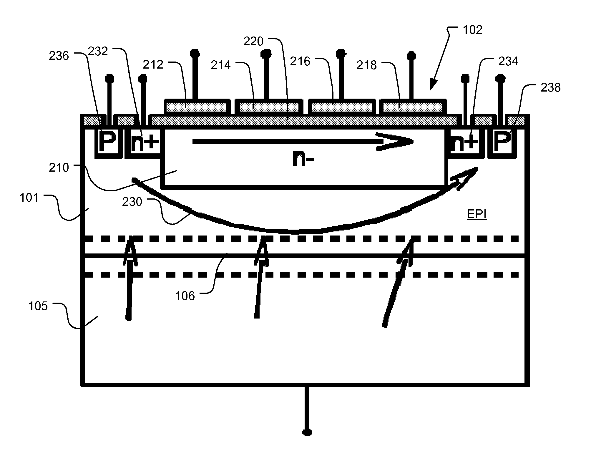
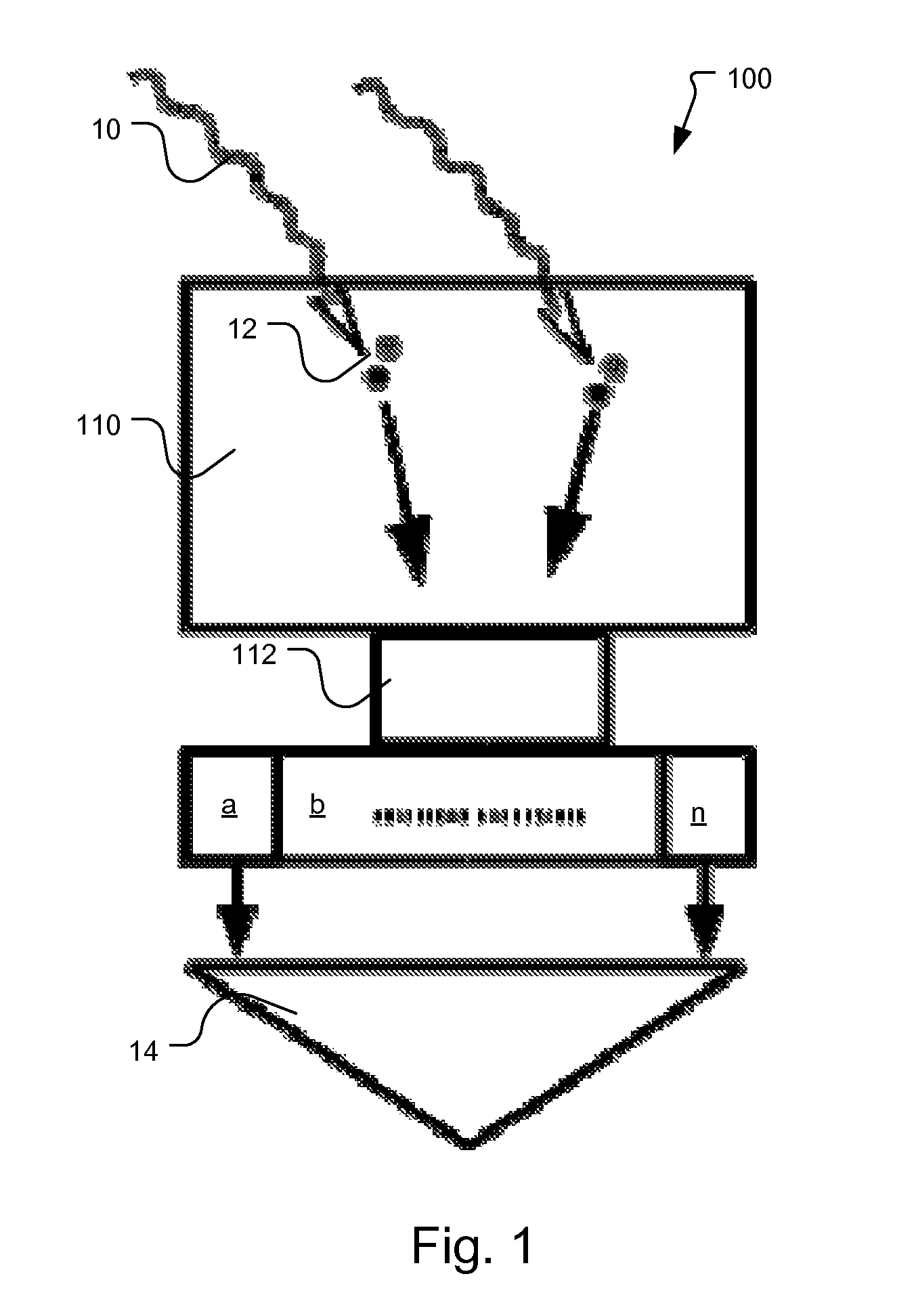
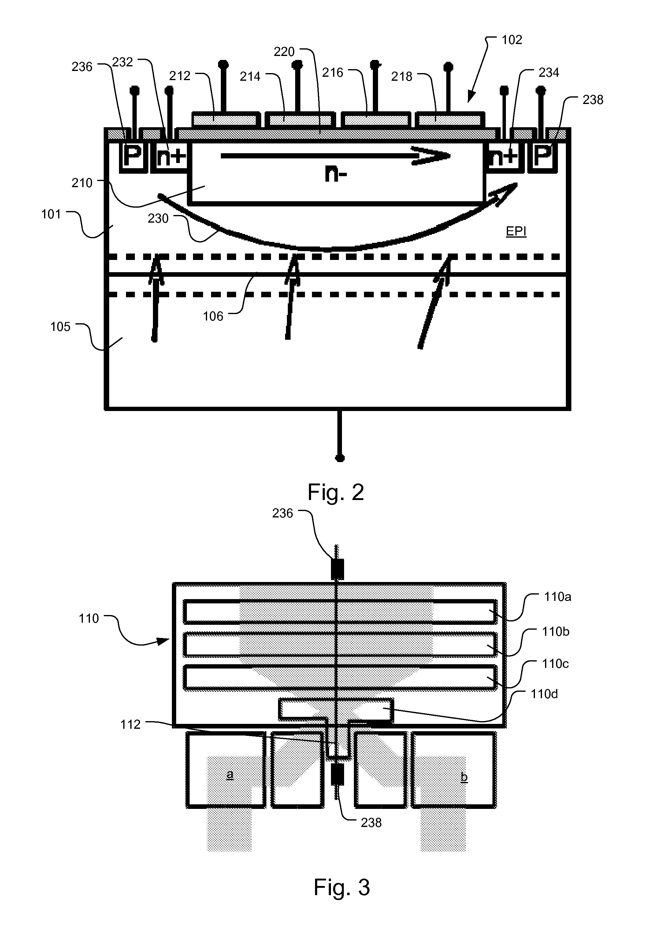
[0031]FIG. 1 is a schematic diagram of a demodulation pixel 100. Photons 10 impinge onto the sensitive area 110 and create electron-hole pairs 12. In general the holes are drained by the substrate and the electrons are used as the charge carriers for the signal processing and extraction of the information. The sensitive region 110 transports the electrons as fast as possible to the demodulation region 112 in order to support high (de)mod...


PUM


Abstract

A demodulation pixel improves the charge transport speed and sensitivity by exploiting two effects of charge transport in silicon in order to achieve the before-mentioned optimization. The first one is a transport method based on the CCD gate principle. However, this is not limited to CCD technology, but can be realized also in CMOS technology. The charge transport in a surface or even a buried channel close to the surface is highly efficient in terms of speed, sensitivity and low trapping noise. In addition, by activating a majority carrier current flowing through the substrate, another drift field is generated below the depleted CCD channel. This drift field is located deeply in the substrate, acting as an efficient separator for deeply photo-generated electron-hole pairs. Thus, another large amount of minority carriers is transported to the diffusion nodes at high speed and detected.

Description

RELATED APPLICATIONS[0001]This application claims the benefit under 35 USC 119(e) of U.S. Provisional Application No. 61 / 233,961, filed on Aug. 14, 2009, which is incorporated herein by reference in its entirety.BACKGROUND OF THE INVENTION[0002]Time resolving or demodulating pixels have different fields of applications. Two typical examples are three dimensional (3D) range imaging and fluorescence lifetime imaging. Basically, in both applications higher in-pixel charge transport speed and higher optical sensitivity lead to more accurate per-pixel measurements.[0003]The time-domain demodulation of modulated light signals at the pixel level requires in all approaches the switching of a photo-generated charge current. It is possible to handle electron as well as hole currents. The common methods, however, use the photo-generated electron currents due to the higher mobility of electrons in the semiconductor material.[0004]Some pixel architectures do the necessary signal processing based...

Claims


Application Information

Patent Timeline
Patent Type & Authority Applications(United States)
IPC IPC(8): H01L31/08
CPCH01L27/14812H01L27/14806
Inventor BUETTGEN, BERNHARDFELBER, JONASLEHMANN, MICHAELOGGIER, THIERRY
Owner AMS SENSORS SINGAPORE PTE LTD
Why Eureka
Try Eureka