Liquid crystal device, method of manufacturing the same, and electronic apparatus

a liquid crystal device and manufacturing method technology, applied in the field of liquid crystal devices, can solve the problems of difficult to realize the reproducibility of a layer suppressing the movement of charges precisely and uniformly, the difficulty of manufacturing an apparatus, and the appearance of electric asymmetry, so as to achieve the effect of preventing charges easily and reliably

Inactive Publication Date: 2011-04-21
SEIKO EPSON CORP
View PDF11 Cites 2 Cited by
  • Summary
  • Abstract
  • Description
  • Claims
  • Application Information

AI Technical Summary

Benefits of technology

[0007]An advantage of some aspects of the invention is that it provides a liquid crystal device, a method of manufacturing the same, and an electroni

Problems solved by technology

Therefore, charges may move in the interface of the liquid crystal and the electrodes, and thus considerable electric asymmetry appears.
Moreover, it is very difficult to realize reproducibility of a layer suppressing movement of charges precisely and uniformly in a vacuum film forming method as in JP-A-2007-

Method used


Image

  • Liquid crystal device, method of manufacturing the same, and electronic apparatus
  • Liquid crystal device, method of manufacturing the same, and electronic apparatus
  • Liquid crystal device, method of manufacturing the same, and electronic apparatus

Examples


Embodiment Construction

[0038]Hereinafter, an embodiment of the invention will be described with reference to the drawings.

Liquid Crystal Device

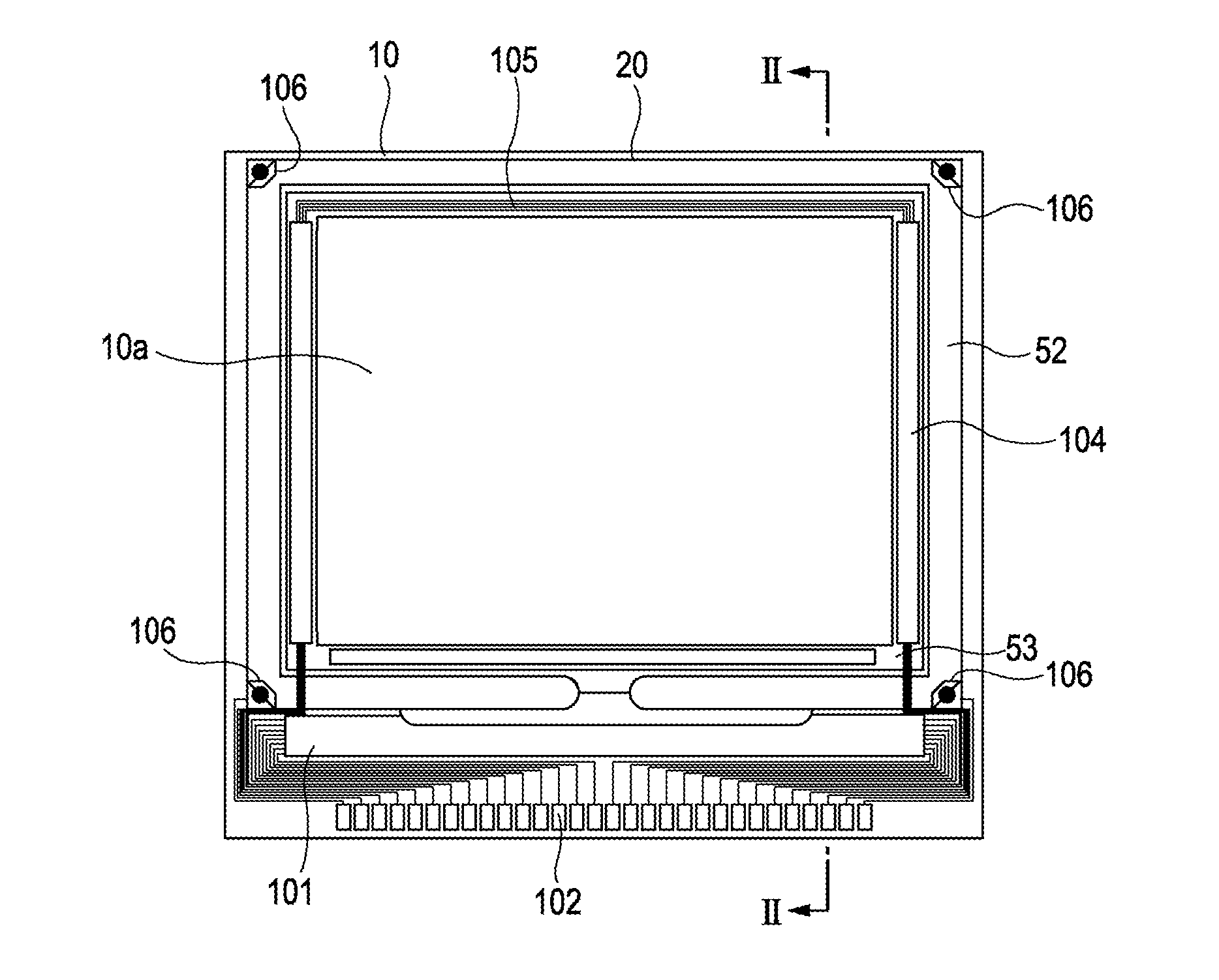
[0039]A liquid crystal device according to an embodiment will be first described with reference to FIGS. 1 to 5. In the embodiment described below, a liquid crystal device with a built-in drive circuit of a TFT (Thin Film Transistor) active matrix drive type will be described as an example of the liquid crystal device according to the invention.

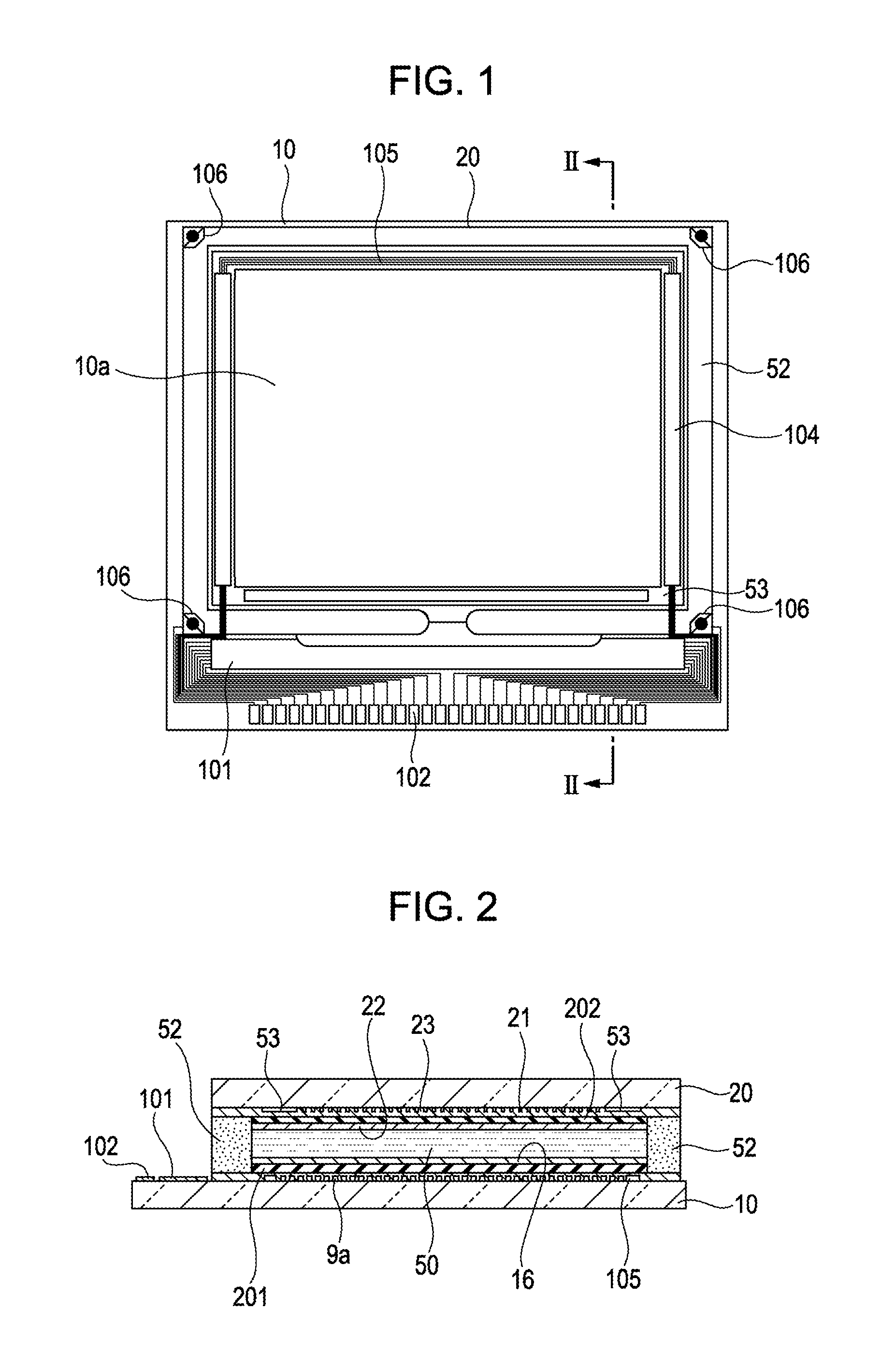
[0040]The overall configuration of the liquid crystal device according to this embodiment will be described with reference to FIGS. 1 and 2. FIG. 1 is a plan view illustrating the overall configuration of the liquid crystal device according to this embodiment. FIG. 2 is a sectional view taken along the line II-II of FIG. 1.

[0041]In FIGS. 1 and 2, a TFT array substrate 10 and a counter substrate 20 which are an example of a “pair of substrates” according to the invention are arranged to be opposite to each other in the liquid...


PUM


Abstract

A liquid crystal device includes: a liquid crystal layer being interposed between a pair of substrates; an electrode disposed on surfaces of at least one of the pair of substrates facing the liquid crystal layer; a self-assembled film disposed to cover the electrode on the side of the liquid crystal layer; and an inorganic alignment film disposed between the self-assembled film and the liquid crystal layer.

Description

BACKGROUND[0001]1. Technical Field[0002]The present invention relates to a liquid crystal device, a method of manufacturing the same, and an electronic apparatus, such as a liquid crystal projector, including the liquid crystal device.[0003]2. Related Art[0004]An example of this kind of liquid crystal device includes a liquid crystal device in which a liquid crystal layer is interposed between inorganic alignment films. In this liquid crystal device, there is a region where a liquid crystal comes into contact with electrodes in the gap portion between the inorganic alignment films. Therefore, charges may move in the interface of the liquid crystal and the electrodes, and thus considerable electric asymmetry appears. Since the electric asymmetry causes a display failure such as flicker or screen burns, various techniques suppressing the electric asymmetry have been suggested.[0005]For example, JP-A-2003-57674 discloses a technique for suppressing the electric asymmetry by covering a ...

Claims


Application Information

Patent Timeline
IPC IPC(8): G02F1/1337
CPCH04N9/3102H04N9/3197G02F1/133345G02F2203/12G02F1/13439G02F1/136259G02F2001/133397G02F1/133734G02F1/133397
Inventor TANAKA, TAKAAKI
Owner SEIKO EPSON CORP
Why Eureka
Try Eureka