Graphene synthesis by chemical vapor deposition

a graphene and chemical vapor deposition technology, applied in chemical vapor deposition coatings, coatings, material nanotechnology, etc., can solve the problems of high cost, difficult and impractical industrial environment implementation, limited graphene size, etc., and achieve the effect of increasing the flow rate of methan

Active Publication Date: 2011-04-21
TEXAS INSTR INC +1
View PDF8 Cites 90 Cited by
  • Summary
  • Abstract
  • Description
  • Claims
  • Application Information

AI Technical Summary

Benefits of technology

[0009]In another embodiment of the present invention, a method for synthesizing graphene films comprises loading a metal or a dielectric onto a substrate into a tube furnace or a cold wall chamber. The method further comprises introducing hydrogen gas at a rate between 1 to 100 sccm into the tube furnace or cold wall chamber. Furthermore, the method comprises heating the substrate to a temperature between 400° C. and 1,400° C. Additionally, the method comprises maintaining the temperature of the substrate to between 400° C. and 1,400° C. for a duration of time between 0.1 to 60 minutes while the hydrogen gas is flowing into the tube furnace or cold wall chamber. In addition, the method comprises introducing methane into the tube furnace or cold wall chamber at a flow rate between 1 to 5,000 sccm at between 10 mTorr to 780 Torr of pressure while reducing the flow rate of hydrogen gas to less than 10 sccm. Furthermore, the method comprises growing graphene from the methane on the metal or dielectric over a period of time between 0.001 to 10 minutes following the introduction of the methane.
[0010]In another embodiment of the present invention, a method for synthesizing graphene films comprises loading a metal or a dielectric onto a substrate into a tube furnace or a cold wall chamber. The method further comprises introducing hydrogen gas at a rate between 1 to 100 sccm into the tube furnace or cold wall chamber at a pressure ranging from 10 mTorr to 2 Torr. In addition, the method comprises heating the substrate to a temperature between 400° C. and 1,400° C. Furthermore, the method comprises maintaining the temperature of the substrate to between 400° C. and 1,400° C. for a duration of time between 0.1 to 60 minutes while the hydrogen gas is flowing into the tube furnace or cold wall chamber. In addition, the method comprises introducing methane into the tube furnace or cold wall chamber at a flow rate between 1 to 5,000 sccm at between 10 mTorr to 780 Ton of pressure while reducing the flow rate of hydrogen gas to less than 10 sccm thereby growing nuclei over a time period between 0.001 to 120 seconds. Additionally, the method comprises increasing the flow rate of methane by between 10 to 5,000 sccm whereby graphene is grown from methane on the metal or dielectric over a period of time between 0.01 to 600 seconds following the introduction of the methane.

Problems solved by technology

However, graphene produced by this method is of very limited size (e.g., at most a few hundred micrometers on the side), very expensive, not scalable, and very difficult and impractical to implement in an industrial environment.
Furthermore, the quality of the graphene produced from this process degrades at the crystallographic step edges.
One major disadvantage of the graphene synthesis on silicon carbide process is that even if it were scalable to large diameter crystals, it is not possible to use it for applications other than just on silicon carbide.

Method used


Image

  • Graphene synthesis by chemical vapor deposition
  • Graphene synthesis by chemical vapor deposition
  • Graphene synthesis by chemical vapor deposition

Examples


Embodiment Construction

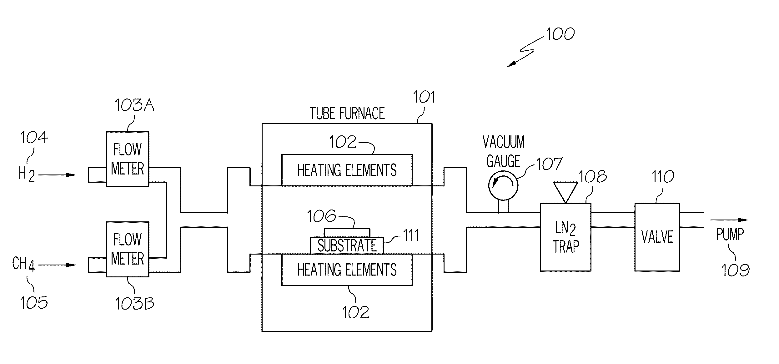
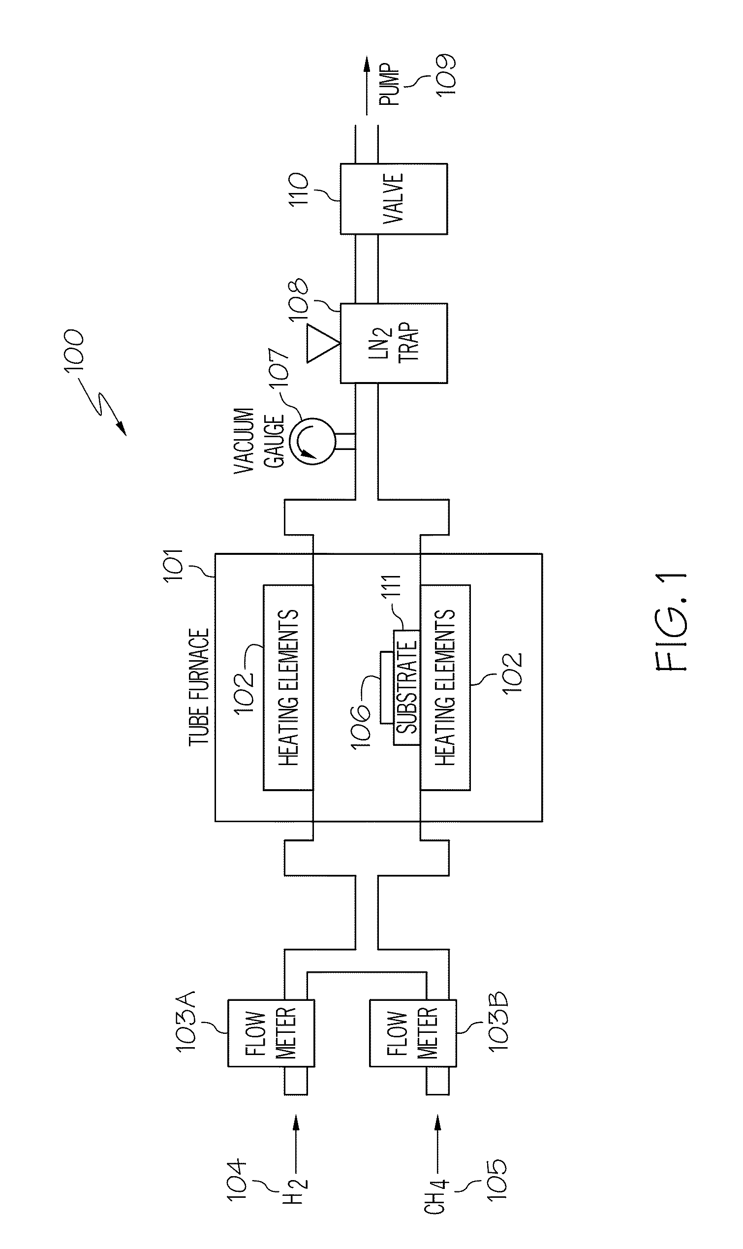
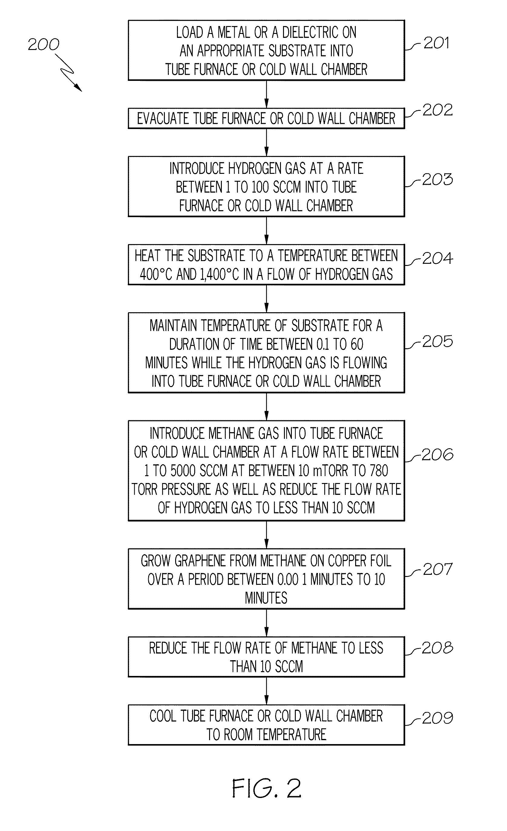
[0017]As discussed in the Background section, currently, large graphene crystallites can be produced by mechanical exfoliation (repeated peeling) of graphite crystals. However, graphene produced by this method is difficult to form and is not at all scalable. Another method for producing graphene is to heat silicon carbide to high temperatures (e.g., much greater than 1,400° C.) to reduce it to graphene. This process produces a sample size that is dependent upon the size of the silicon carbide substrate used. The face of the silicon carbide used for graphene creation highly influences the thickness, mobility and carrier density of the graphene. While this process is scalable, it is limited to applications where a silicon carbide substrate is part of the device. Large area graphene films required by many applications will be difficult if not impossible to fulfill using this technique. Therefore, there is a need in the art for the synthesis of standalone graphene films with properties ...


PUM

PropertyMeasurementUnit
temperatureaaaaaaaaaa
pressureaaaaaaaaaa

Abstract

Processes for synthesizing graphene films. Graphene films may be synthesized by heating a metal or a dielectric on a substrate to a temperature between 400° C. and 1,400° C. The metal or dielectric is exposed to an organic compound thereby growing graphene from the organic compound on the metal or dielectric. The metal or dielectric is later cooled to room temperature. As a result of the above process, standalone graphene films may be synthesized with properties equivalent to exfoliated graphene from natural graphite that is scalable to size far greater than that available on silicon carbide, single crystal silicon substrates or from natural graphite.

Description

CROSS-REFERENCE TO RELATED APPLICATIONS[0001]This application is related to the following commonly owned co-pending U.S. patent application:[0002]Provisional Application Ser. No. 61 / 253,616, “Synthesizing Graphene With Improved Conductivity Due to Increasing Domain Size and Reducing Domain Boundaries,” filed Oct. 21, 2009, and claims the benefit of its earlier filing date under 35 U.S.C. §119(e).TECHNICAL FIELD[0003]The present invention relates to making graphene, and more particularly to synthesizing graphene films with improved conductivity by controlling the graphene domain size and decreasing the density of the domain boundaries.BACKGROUND OF THE INVENTION[0004]Graphene is a one-atom-thick planar sheet of sp2-bonded carbon atoms that are densely packed in a honeycomb crystal lattice. The carbon-carbon bond length in graphene is about 0.142 nm. Graphene is the basic structural element of some carbon allotropes including graphite, carbon nanotubes and fullerenes.[0005]Currently, ...

Claims


Application Information

Patent Timeline
Patent Type & Authority Applications(United States)
IPC IPC(8): C23C16/44C23C16/26
CPCB82Y30/00C23C16/26C01B31/0453B82Y40/00C01B32/186
Inventor COLOMBO, LUIGILI, XUESONGRUOFF, RODNEY S.
Owner TEXAS INSTR INC
Why Eureka
Try Eureka