Pressure-sensitive adhesive film and back-grinding method using the same

a technology of pressure-sensitive adhesive and backgrinding method, which is applied in the direction of film/foil adhesives, solid-state devices, synthetic resin layered products, etc., can solve the problems of affecting the cutting efficiency of wafers, so as to improve the cutting efficiency and reduce the cost of production. , the effect of superior cuttability and adhesion

Inactive Publication Date: 2011-04-21
LG CHEM LTD
View PDF3 Cites 9 Cited by
  • Summary
  • Abstract
  • Description
  • Claims
  • Application Information

AI Technical Summary

Benefits of technology

[0013]In the present invention, a pressure-sensitive adhesive film is provided, which can remarkably raise the efficiency of production in semiconductor manufacturing processes such as wafer backgrinding, since it has superior cuttability and adhesion properties in the semiconductor manufacturing processes, and an excellent cushioning property. Moreover, the present invention also provides a pressure-sensitive adhesive film having superior peeling and re-peeling properties, that provides wettability to the wafer while providing excellent water resistance, and a backgrinding method using the pressure-sensitive adhesive film. According to the present invention, when the protective film is adhered to the wafer and cut according t

Problems solved by technology

Moreover, as the diameter of the wafer increases, wafer damage such as wafer contamination and cracks frequently occur during the backgrinding process.
However, even though the pressure-sensitive adhesive films suggested in the foregoing conventional techniques can prevent damage to the wafer during back surface grinding, their properties are si

Method used


Image

  • Pressure-sensitive adhesive film and back-grinding method using the same
  • Pressure-sensitive adhesive film and back-grinding method using the same
  • Pressure-sensitive adhesive film and back-grinding method using the same

Examples


example 1

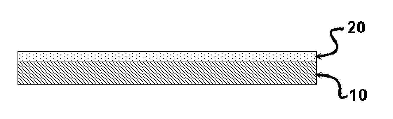
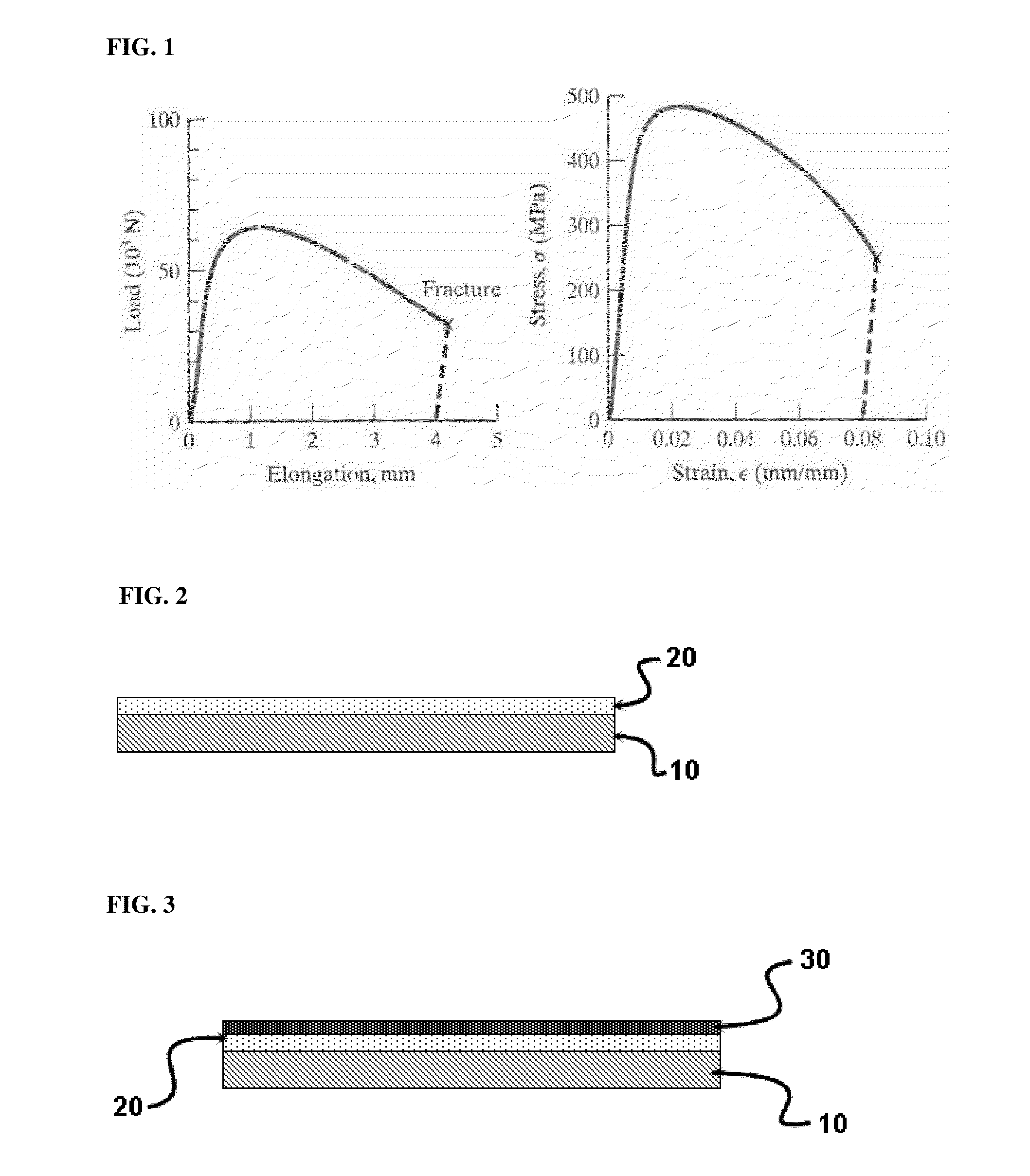
[0070]A monomer mixture (100 parts by weight) comprising isobonyl acrylate, methyl acrylate, ethyl acrylate, n-butyl acrylate and 2-hydroxyethyl acrylate was prepared such that 5 parts by weight of isobonyl acrylate (IBOA) were contained in the mixture, and the glass transition temperature of the resin prepared from the mixture was −25° C. Then, the monomer mixture was polymerized to prepare an acrylic pressure-sensitive adhesive resin having a solid content of 45 weight %. Next, an isocyanate cross-linking agent was added to the prepared pressure-sensitive adhesive resin in an amount of 2 parts by weight, relative to 100 parts by weight of the pressure-sensitive adhesive resin. The resultant was applied to an ethylene-acetic acid vinyl copolymer film (EVA) having a toughness of 137 Kg·mm, a storage modulus of 5×10⁷ Pa at 20° C., an elongation of 434%, a tensile strength of 139 Kg / cm2, and then dried, thus preparing a pressure-sensitive adhesive film. The toughness, storage modulus,...


PUM

PropertyMeasurementUnit
Temperatureaaaaaaaaaa

Abstract

The present invention relates to a pressure-sensitive adhesive film and a semiconductor wafer backgrinding method using the same. The present invention provides a pressure-sensitive adhesive film capable of remarkably improving production efficiency in a wafer backgrinding of a semiconductor manufacturing process due to its superior cutting and adherence properties in the semiconductor manufacturing process and an excellent cushioning property. Moreover, the present invention also provides a pressure-sensitive adhesive film having superior peeling and re-peeling properties and wettability to the wafer while providing excellent water resistance, and a backgrinding method using the pressure-sensitive adhesive film.

Description

TECHNICAL FIELD[0001]The present invention relates to a pressure-sensitive adhesive film and a backgrinding method.BACKGROUND ART[0002]With the recent tendency towards miniaturization and weight-reduction of electronic products, there is an increasing demand for leadless, thin-film, and high-integration chip semiconductor packages. To meet the demand, a need for large-diameter thin-film wafers included in the semiconductor packages is also increasing.[0003]In order to effectively cope with the tendency towards large diameter thin-film semiconductor wafers, it is important to precisely control a backgrinding process, which is a wafer grinding process, and a dicing process, which is a reorganizing process. To this end, high-performance techniques capable of controlling these processes are required. The backgrinding process is a process of mechanically or chemically polishing the surface of a wafer having a high-integration interconnection circuit to make the wafer thin. In this proces...

Claims


Application Information

Patent Timeline
IPC IPC(8): C09J7/02B24B1/00B32B5/00C09J133/08C09J133/10B32B33/00C09J7/22
CPCC09J7/026Y10T428/1476C09J2423/006C09J2427/006C09J2433/00C09J2467/006C09J2475/006H01L21/6835H01L21/6836H01L2221/68327H01L2221/68386Y10T428/2852Y10T428/28Y10T428/2891Y10T428/266Y10T428/2887Y10T428/264C09J2203/326C09J7/22
Inventor KIM, SE RABAEK, YOON JEONKIM, JAN SOONSON, HYUN HEEHONG, JONG WANPARK, HYUN WOO
Owner LG CHEM LTD
Why Eureka
Try Eureka