Method and structure for silicon nanocrystal capacitor devices for integrated circuits

a technology of integrated circuits and capacitors, which is applied in the field of integrated circuits, can solve the problems of reducing the yield of silicon nanocrystal capacitors, and reducing the cost of integrated circuit or chip fabrication facilities, so as to improve the capacitor structure, improve the yield of dies per wafer, and facilitate use

Inactive Publication Date: 2011-04-28
SEMICON MFG INT (SHANGHAI) CORP +1
View PDF8 Cites 9 Cited by
  • Summary
  • Abstract
  • Description
  • Claims
  • Application Information

AI Technical Summary

Benefits of technology

[0008]In a specific embodiment, the present invention provides a semiconductor device, including a capacitor structure, e.g., stack capacitor, trench capacitor, or other like structure physically and/or functionally. The device has a first electrode member (e.g., doped polysilicon, combinations of conductive materials, metals), which has a first length and a first width. The device also has a second electrode member (e.g., doped polysilicon, combinations of conductive materials, metals) coupled to the first electrode member, which has a second length and a second width. A capacitor dielectric material is provided between the first electrode member and the second electrode member according to a specific embodiment. Depending upon the embodiment, the capacitor dielectric is made of a suitable material or materials such as Al2O3, HfO2, silicon nitride, silicon oxynitride, ONO (silicon oxide on silicon nitride on silicon oxide) stack, Al2O3/HfO2, AlNyOx, ZrO2, any combinations of these, and the like. These materials can be deposited using ALD, MOCVD, UHV-PVD, reactive sputtering and/or chemical solution according to a specific embodiment. The device includes a plurality silicon nanocrystals spatially disposed in an area associated with the first width and the first length of the first electrode member. Each one of the silicon nanocrystals has a size of about 20 nanometers and less according to a specific embodiment. In other embodiments, the nanocrystals can have an average size of about 2 nanometers and less, but can be other dimensions as well.
[0009]In an alternative specific embodiment, the present invention provides a method for fabricating semiconductor devices. The method includes providing a semiconductor substrate, e.g., silicon wafer. The method includes forming a first electrode member coupled to the semiconductor substrate. The first electrode member has a first length and a first width according to a specific embodiment. The method includes forming a first capacitor dielectric material overlying the first electrode member. Depending upon the embodiment, the capacitor dielectric material is ma

Problems solved by technology

An integrated circuit or chip fabrication facility can cost hundreds of millions, or even billions, of U.S. dollars.
Making devices smaller is very challenging, as each process used in integrated fabrication has a limit.
Additionally, as devices require faster and faster designs, process limitations exist with certain conventional processes and materials.
Although there have been si

Method used


Image

  • Method and structure for silicon nanocrystal capacitor devices for integrated circuits
  • Method and structure for silicon nanocrystal capacitor devices for integrated circuits
  • Method and structure for silicon nanocrystal capacitor devices for integrated circuits

Examples


Embodiment Construction

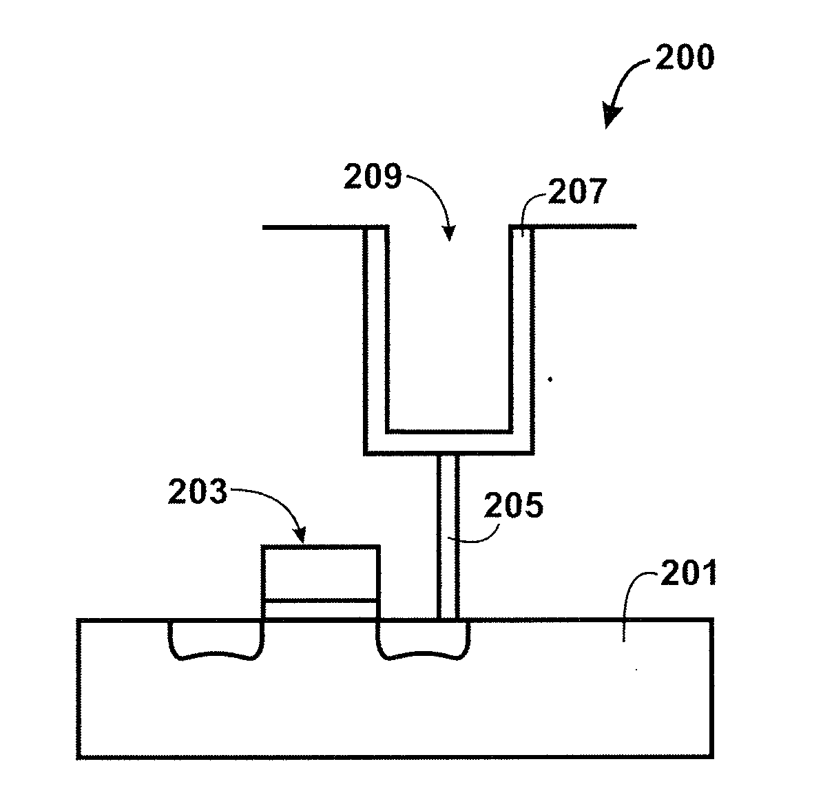
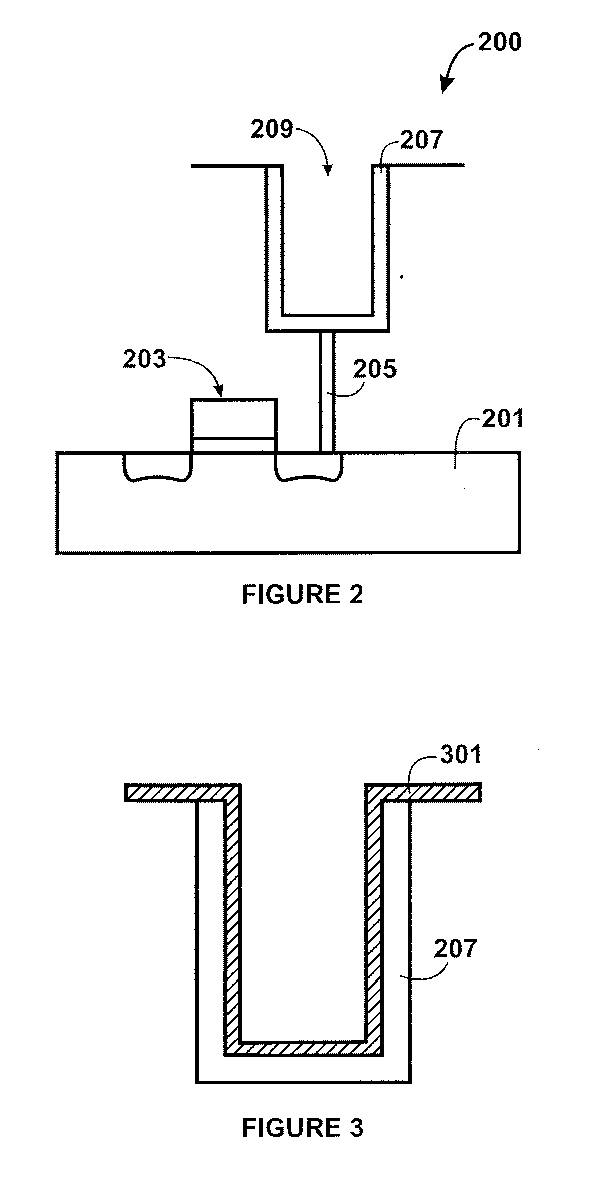
[0015]According to the present invention, techniques for processing integrated circuits for the manufacture of semiconductor devices are provided. More particularly, the invention provides a method and device for manufacturing a stack capacitor of a dynamic random access memory device, commonly called DRAMs, but it would be recognized that the invention has a much broader range of applicability. For example, the invention can be applied to other devices having stack capacitor designs and / or like structures.

[0016]A method for manufacturing a capacitor device according to an embodiment of the present invention may be outlined as follows.

[0017]1. Provide a semiconductor substrate, e.g., silicon wafer;

[0018]2. Form a plurality of transistor structures overlying the substrate;

[0019]3. Form a first electrode member coupled to one of the transistor structures on the semiconductor substrate, the first electrode member having a first length and a first width;

[0020]4. Form a first a capacitor...


PUM


Abstract

An improved semiconductor device, including a capacitor structure. The device has a first electrode member, which has a first length and a first width. The device also has a second electrode member, which has a second length and a second width. Additionally, the device includes a capacitor dielectric material provided between the first electrode member and the second electrode member according to a specific embodiment. Depending upon the embodiment, the capacitor dielectric material is made of a suitable material or materials such as Al2O3, HfO2, SiN, NO, Al2O3/HfO2, AlNyOx, ZrO2, any combinations of these, and the like. The device further includes a plurality of silicon nanocrystals spatially disposed in an area associated with the first width and the first length of the first electrode member. Each one of the nanocrystals has a size of about 20 nanometers and less according to a specific embodiment.

Description

CROSS-REFERENCES TO RELATED APPLICATIONS[0001]This application claims priority to Chinese Application No. 200910197614.2, filed on Oct. 23, 2009, commonly assigned herewith and incorporated in its entirety by reference herein for all purposes.BACKGROUND OF THE INVENTION[0002]The present invention is directed to integrated circuits and their processing for the manufacture of semiconductor devices. More particularly, the invention provides a method and device for manufacturing a stack capacitor of a dynamic random access memory device, commonly called DRAMs, but it would be recognized that the invention has a much broader range of applicability. For example, the invention can be applied to other devices having stack capacitor designs and / or like structures.[0003]Integrated circuits have evolved from a handful of interconnected devices fabricated on a single chip of silicon to millions of devices. Conventional integrated circuits provide performance and complexity far beyond what was o...

Claims


Application Information

Patent Timeline
IPC IPC(8): H01L27/08H01L21/02
CPCB82Y10/00H01L28/84H01L27/10852H10B12/033
Inventor FUMITAKE, MIENO
Owner SEMICON MFG INT (SHANGHAI) CORP
Why Eureka
Try Eureka