Wafer-shaped optical apparatus and manufacturing method thereof, electronic element wafer module, sensor wafer module, electronic element module,sensor module, and electronic information device

Inactive Publication Date: 2011-04-28
SHARP KK
View PDF10 Cites 36 Cited by
  • Summary
  • Abstract
  • Description
  • Claims
  • Application Information

AI Technical Summary

Benefits of technology

[0038]Therefore, by using a base material such as glass, contraction of an overall resin does not influence on optical parts such as a resin lens. Such a base material is not used in the optical parts such as a resin lens, but a single optical resin material is used so as to obtain high optical accuracy.
[0039]According to the present invention as described above, a glass substrate with holes is used as a base material, so that contraction of resin can be inhibited during the manufacturing and a wafer-shaped lens module can be formed with

Problems solved by technology

However, there is no such technique currently existing for mounting a non-spherical glass ball into the hole 102 while controlling the glass ball for securing a desired lens characteristic.
Thus, it is not possible to manufacture a non-spherical lens using the subject method.
It is also difficult to grind the glass ball 103 equally in such a m

Method used


Image

  • Wafer-shaped optical apparatus and manufacturing method thereof, electronic element wafer module, sensor wafer module, electronic element module,sensor module, and electronic information device
  • Wafer-shaped optical apparatus and manufacturing method thereof, electronic element wafer module, sensor wafer module, electronic element module,sensor module, and electronic information device
  • Wafer-shaped optical apparatus and manufacturing method thereof, electronic element wafer module, sensor wafer module, electronic element module,sensor module, and electronic information device

Examples


embodiment 1

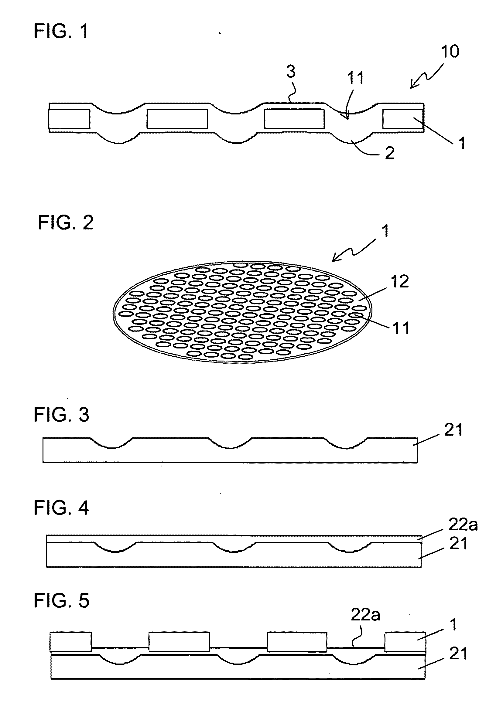
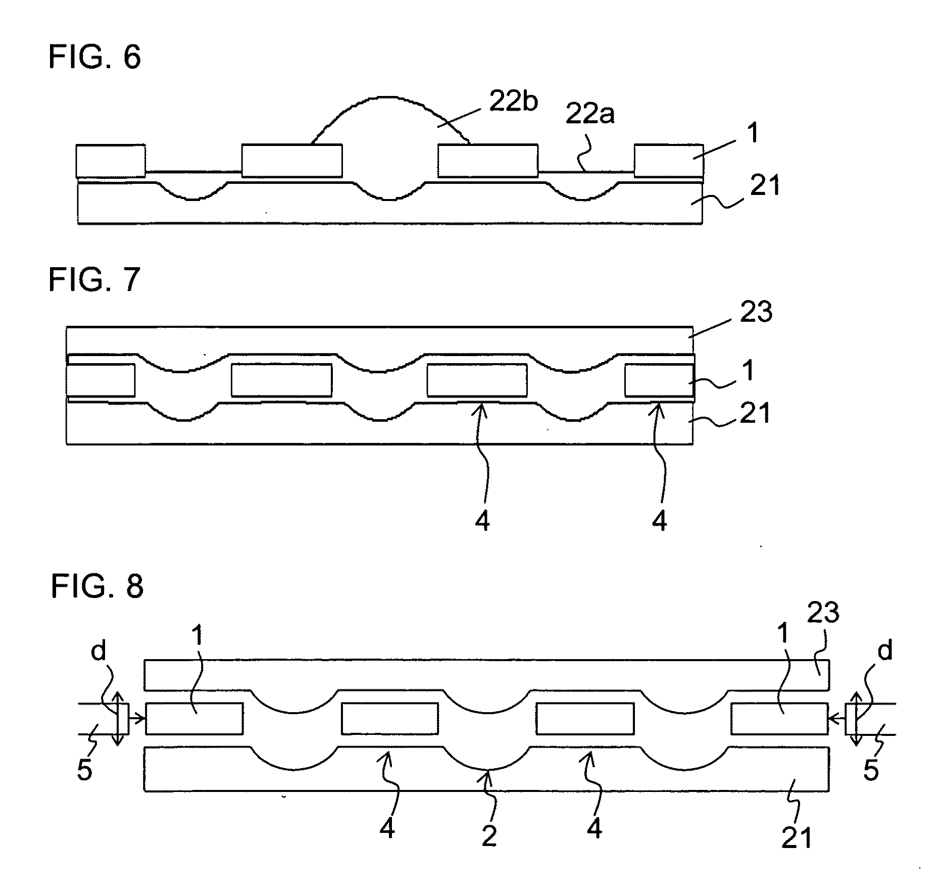
[0094]FIG. 1 is a partial longitudinal cross sectional view schematically illustrating an exemplary essential structure of a lens module according to Embodiment 1 of the present invention.

[0095]In FIG. 1, a lens module 10 functions as a wafer-shaped optical apparatus according to Embodiment 1. The lens module 10 includes: a glass substrate 1 as a base material (framework) with a plurality of holes 11 formed therein; a resin lens 2 formed to correspond to each of the plurality of holes 11; and a peripheral resin section 3 made with the same resin material as the resin lens 2 and formed on upper and lower surfaces of the glass substrate 1 in the periphery of the resin lens 2.

[0096]As illustrated in FIG. 2, the glass substrate 1 is a thin disk in shape with a light shielding chromium plating 12 provided on a front surface side thereof. The glass substrate 1 further includes a plurality of holes 11 formed therein in a matrix at equal intervals. The glass substrate 1 has an effect of inh...

embodiment 2

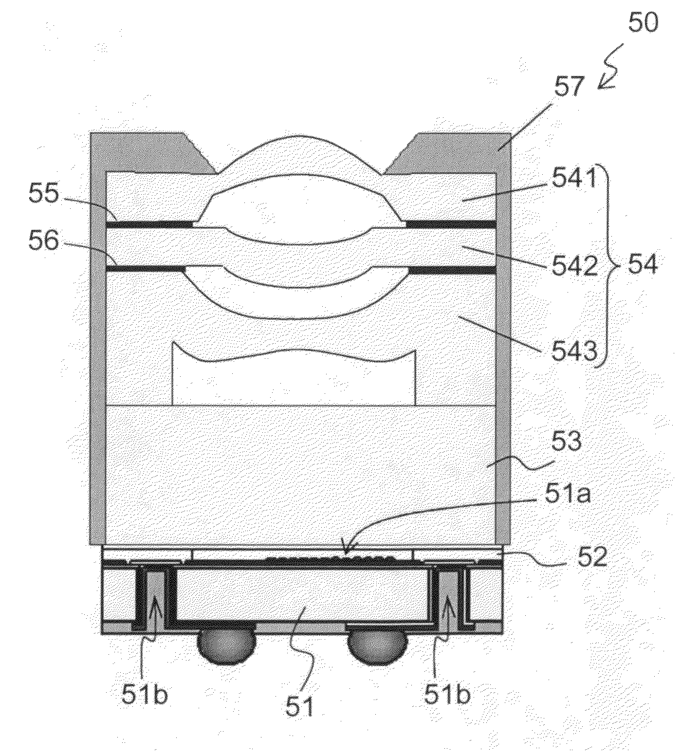
[0112]FIG. 16 is a longitudinal cross sectional view illustrating an exemplary essential structure of a sensor module according to Embodiment 2 of the present invention.

[0113]In FIG. 16, a sensor module 50 according to Embodiment 2 includes: a through wafer 51 provided with an image capturing element 51a and a through hole 51b connecting a front surface and a back surface thereof, the image capturing element 51a including a plurality of light receiving sections, that is, photoelectric conversion sections (photodiodes) corresponding to a plurality of pixels, provided on the front surface thereof, as an electronic element; a resin adhesive layer 52 formed around the image capturing element 51a of the through wafer 51; a glass plate 53 as a cover glass covering the resin adhesive layer 52; a lens plate 54 provided on the glass plate 53 and in which a plurality of lens plates 541 to 543 are layered as optical elements for focusing incident light on the image capturing element 51a; lens ...

embodiment 3

[0122]FIG. 17 is a block diagram illustrating an exemplary diagrammatic structure of an electronic information device according to Embodiment 3 of the present invention, including a sensor module 50 according to Embodiment 2 of the present invention used in an image capturing section thereof.

[0123]In FIG. 17, an electronic information device 90 according to Embodiment 3 of the present invention includes: a solid-state image capturing apparatus 91 for performing various signal processing on an image capturing signal from the sensor module 50 according to Embodiment 2 so as to obtain a color image signal; a memory section 92 (e.g., recording media) for data-recording a color image signal from the solid-state image capturing apparatus 91 after predetermined signal processing is performed on the color image signal for recording; a display section 93 (e.g., a liquid crystal display apparatus) for displaying the color image signal from the solid-state image capturing apparatus 91 on a dis...


PUM

PropertyMeasurementUnit
Thicknessaaaaaaaaaa
Shapeaaaaaaaaaa
Transparencyaaaaaaaaaa

Abstract

A single material is used for an optical member, such as a lens, to obtain high optical accuracy. A glass substrate with a plurality of holes is used as a base material (framework), and overall resin contraction occurred during manufacturing is restrained and a wafer-shaped lens module having a plurality of resin lenses with high dimensional accuracy can be formed. Further, variation in the thickness of the glass substrate is absorbed by lens resin formed on the glass substrate, and the thickness of a flange section can be controlled accurately and variation between resin lenses can also be controlled accurately when layered. Further, a lens portion of the resin lens is made only of a single lens resin, and the refractive index can be maintained even, the designing can be facilitated, and the thickness can be controlled accurately to manufacture a condensing lens with high accuracy.

Description

TECHNICAL FIELD[0001]The present invention relates to a wafer-shaped optical apparatus comprised of a plurality of lenses for focusing incident light, or a plurality of optical functional elements for directing and reflecting straight output light and refracting and guiding incident light in a predetermined direction, and a method for manufacturing the wafer-shaped optical apparatus; an electronic element wafer module including a plurality of image capturing elements modularized (integrated) therein, the image capturing elements having a plurality of light receiving sections for performing a photoelectric conversion on and capturing an image of image light from a subject, corresponding to respective lenses, or an electronic element wafer module including a plurality of light emitting elements for generating output light and light receiving elements for receiving incident light, corresponding to respective optical functional elements, modularized (integrated) therein; an electronic e...

Claims


Application Information

Patent Timeline
IPC IPC(8): H04N5/335H01L31/0232G02B1/10B32B3/10G02B1/12B29D11/00G02B3/00
CPCG02B13/0035G02B13/0085H01L27/14618Y10T428/24777H01L27/14685H04N5/2254H04N5/2257H01L27/14625H01L2224/13H01L27/14632H01L27/14687H01L27/14623H04N23/57
Inventor HASEGAWA, MASAHIRO
Owner SHARP KK
Why Eureka
Try Eureka