Photovoltaic polarizing element and method of manufacturing the same

a technology of photovoltaic polarizing elements and manufacturing methods, which is applied in the direction of sustainable manufacturing/processing, instruments, and final product manufacturing, etc., can solve the problem that the majority of the power consumed by the whole liquid crystal display is consumed by the backligh

Inactive Publication Date: 2011-04-28
CASIO COMPUTER CO LTD
View PDF8 Cites 6 Cited by
  • Summary
  • Abstract
  • Description
  • Claims
  • Application Information

AI Technical Summary

Benefits of technology

[0009]According to an aspect of the invention, a photovoltaic polarizing element includes a first transparent electrode formed on a first transparent substrate; an electron collector formed on the first transparent electrode; dichroic dye molecules arranged in and / or on the electron collector and aligned in a predetermined direction; a second transparent electrode formed on a second transparent substrate, the second transparent electrode and the electron collector facing each other with a gap having a predetermined thickness; and an electron supplier arranged between the first transparent electrode and the second transparent electrode so as to contact the first transparent electrode and the dichroic dye molecules, wherein an energy level of the dichroic dye molecules in an excited state is higher than an energy level of the electron collector, and the energy level of the dichroic dye molecules in a ground state is lower than an energy level of the electron supplier.

Problems solved by technology

In addition, most of power to be consumed by the whole liquid crystal display is consumed by the backlight.

Method used


Image

  • Photovoltaic polarizing element and method of manufacturing the same
  • Photovoltaic polarizing element and method of manufacturing the same
  • Photovoltaic polarizing element and method of manufacturing the same

Examples


Embodiment Construction

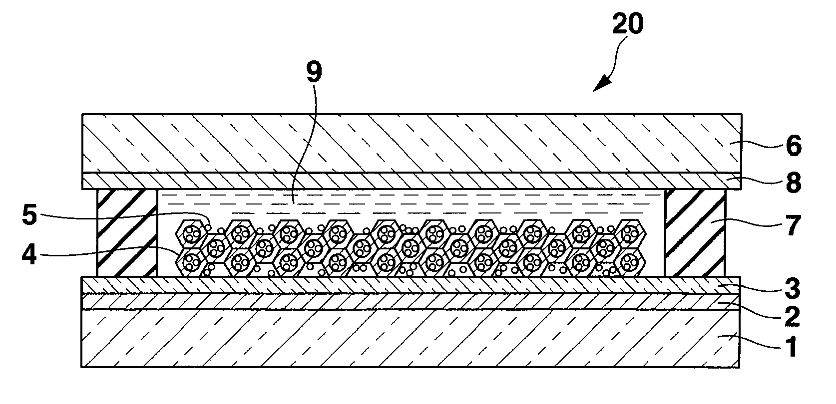
[0019]An embodiment of the present invention will now be described with reference to the accompanying drawings. FIGS. 1 and 2 illustrate a schematic structure of a photovoltaic polarizing element according to this embodiment. As shown in FIGS. 1 and 2, a first transparent conductive film 2 is formed on a first transparent substrate 1. The first transparent substrate 1 may include, for example, glass or a heat-resistant resin. The first transparent conductive film 2 may include, for example, indium tin oxide (ITO) or tin oxide (SnO2). An alignment film 3 made of a polymeric thin film of, for example, polyimide is formed on the surface of the first transparent conductive film 2. A porous layer 4 having cylindrical pores which are aligned in a predetermined direction is formed on the alignment film 3. As the material of the porous layer 4, an oxide semiconductor is preferably used. Out of the oxide semiconductors, particularly, titanium oxide, zinc oxide, tin oxide, tungsten oxide, nio...


PUM

PropertyMeasurementUnit
transparentaaaaaaaaaa
thicknessaaaaaaaaaa
energy levelaaaaaaaaaa

Abstract

A photovoltaic polarizing element includes a first transparent electrode, an electron collector, dichroic dye molecules, a second transparent electrode and an electron supplier. The first transparent electrode is formed on a first transparent substrate. The electron collector is formed on the first transparent electrode. The dichroic dye molecules are arranged in and/or on the electron collector and aligned in a predetermined direction. The second transparent electrode is formed on a second transparent substrate. The electron collector and the second transparent electrode face each other with a gap having a predetermined thickness. The electron supplier arranged between the first transparent electrode and the second transparent electrode. An energy level of the dichroic dye molecules in an excited state is higher than that of the electron collector, and the energy level of the dichroic dye molecules in a ground state is lower than that of the electron supplier.

Description

CROSS-REFERENCE TO RELATED APPLICATIONS[0001]This application is based upon and claims the benefit of priority from prior Japanese Patent Application No. 2009-243670, filed Oct. 22, 2009, the entire contents of which are incorporated herein by reference.BACKGROUND OF THE INVENTION[0002]1. Field of the Invention[0003]The present invention relates to a photovoltaic polarizing element and a method of manufacturing the same.[0004]2. Description of the Related Art[0005]Generally, a polarizing plate passes only polarized light in a specific plane of oscillation. At this time, light components that have not passed through the polarizing plate are absorbed, and most of the luminous energy is dissipated as thermal energy.[0006]As an example, energy consumption of a liquid crystal display will be explained. A liquid crystal display includes a liquid crystal panel formed by sandwiching a liquid crystal layer between two polarizing plates. The liquid crystal display displays an image by control...

Claims


Application Information

Patent Timeline
Patent Type & Authority Applications(United States)
IPC IPC(8): G02F1/1335H01L31/04B32B38/08
CPCY02E10/542G02F1/133528Y10T428/1041G02F2001/13324H01G9/2068C09K2323/031Y02P70/50G02F1/13324
Inventor YOSHIDA, MAMORUYOSHIDA, TETSUSHI
Owner CASIO COMPUTER CO LTD
Why Eureka
Try Eureka