Method of Forming Mono-Crystalline Germanium or Silicon Germanium

a mono-crystalline, germanium or silicon germanium technology, applied in the field of epitaxial devices, can solve the problems of reducing the size of many devices, and scaling down

Inactive Publication Date: 2011-04-28
INTERUNIVERSITAIR MICRO ELECTRONICS CENT (IMEC VZW) +1
View PDF17 Cites 76 Cited by
  • Summary
  • Abstract
  • Description
  • Claims
  • Application Information

AI Technical Summary

Benefits of technology

[0027]In some embodiments, removing at least a portion of the insulating regions may comprise etching the insulating regions. In some embodime

Problems solved by technology

The scaling down of planar bulk complementary metal-oxide-semiconductor (CMOS) devices has become a major challenge in the semiconductor industry.
While the sizes of many devices has been reduced (and corresponding performances have been improved), device architectures below the 90 nm range remain a challenge.
Additionally, in the described method, th

Method used


Image

  • Method of Forming Mono-Crystalline Germanium or Silicon Germanium
  • Method of Forming Mono-Crystalline Germanium or Silicon Germanium
  • Method of Forming Mono-Crystalline Germanium or Silicon Germanium

Examples


Embodiment Construction

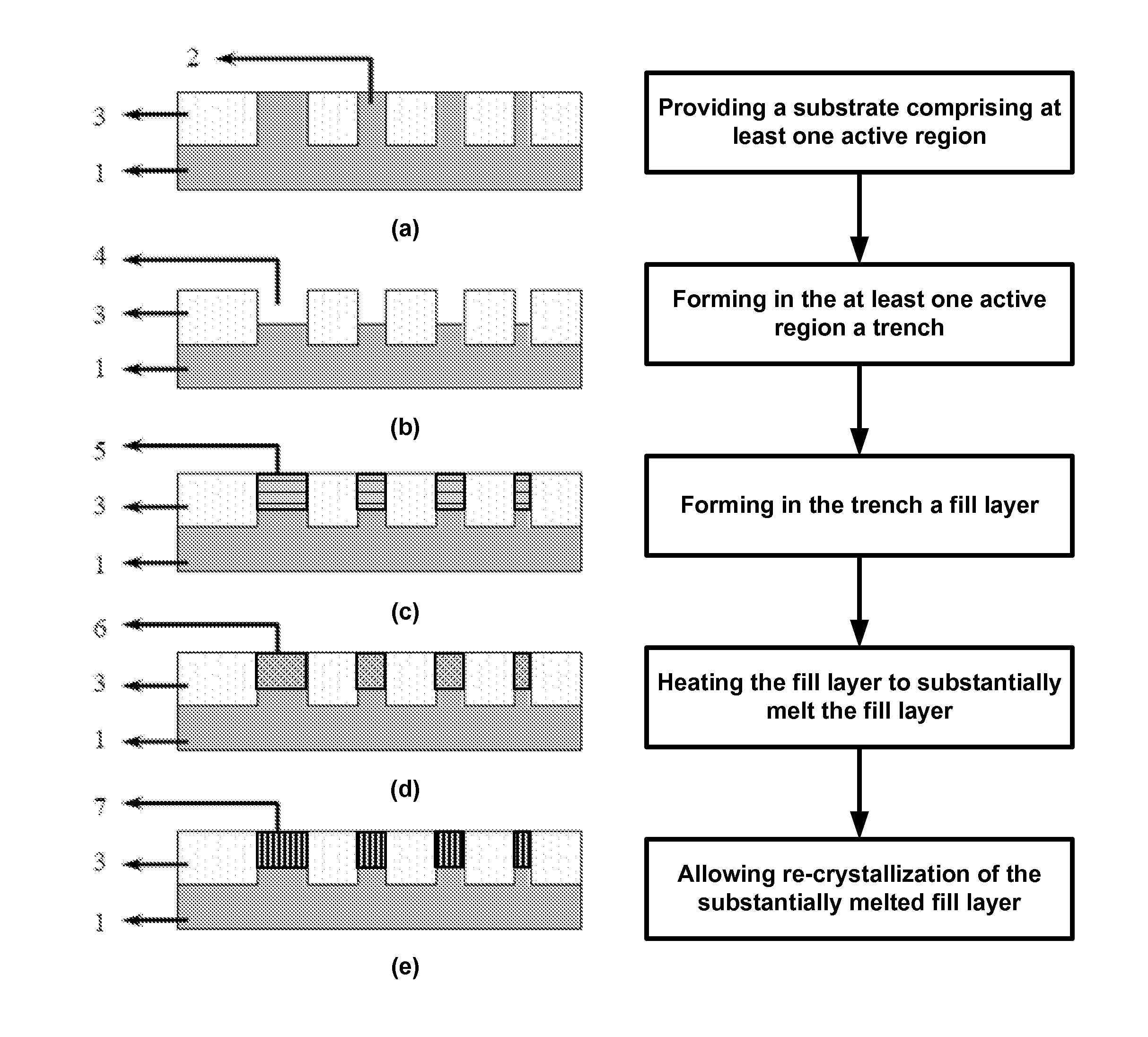
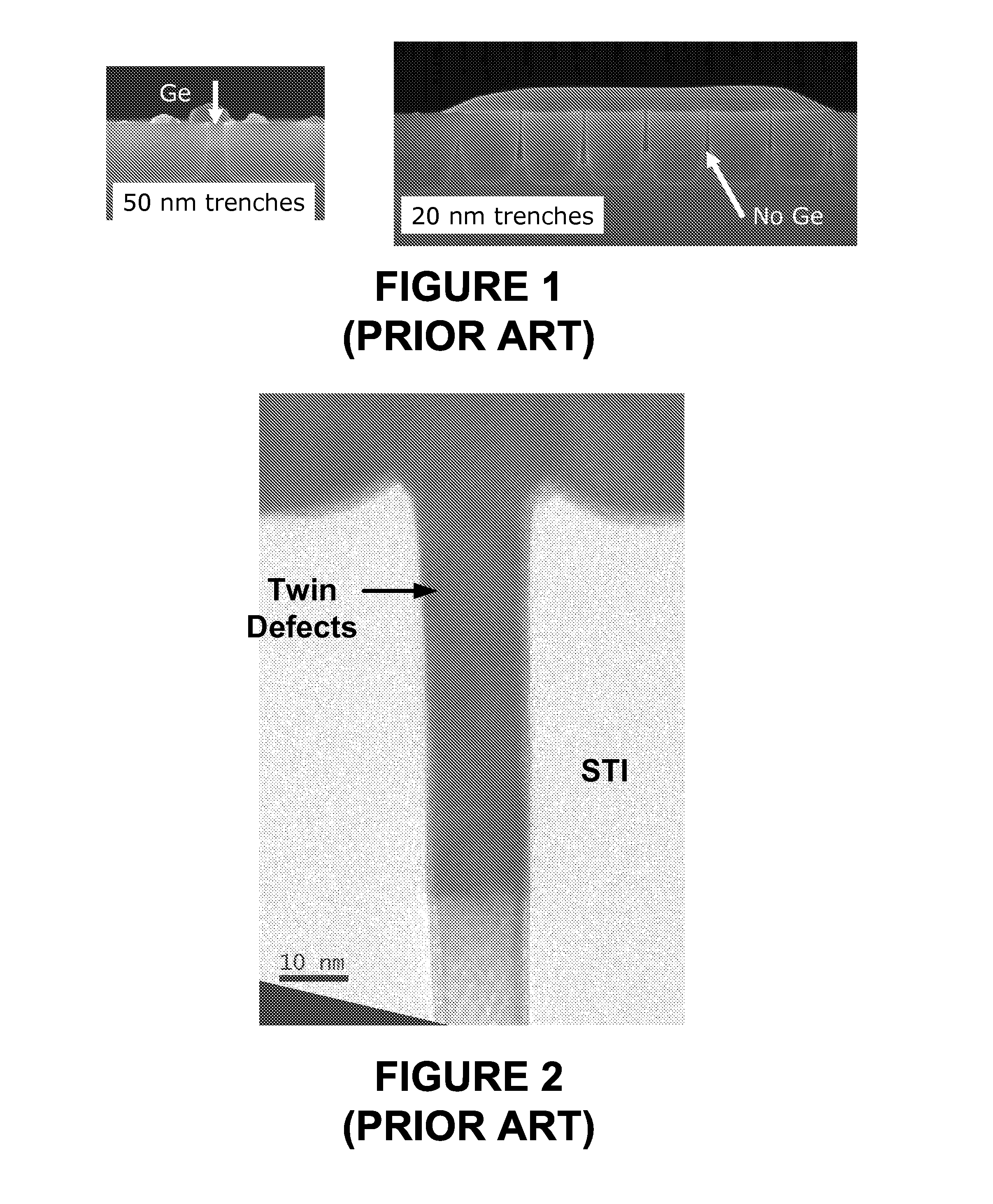
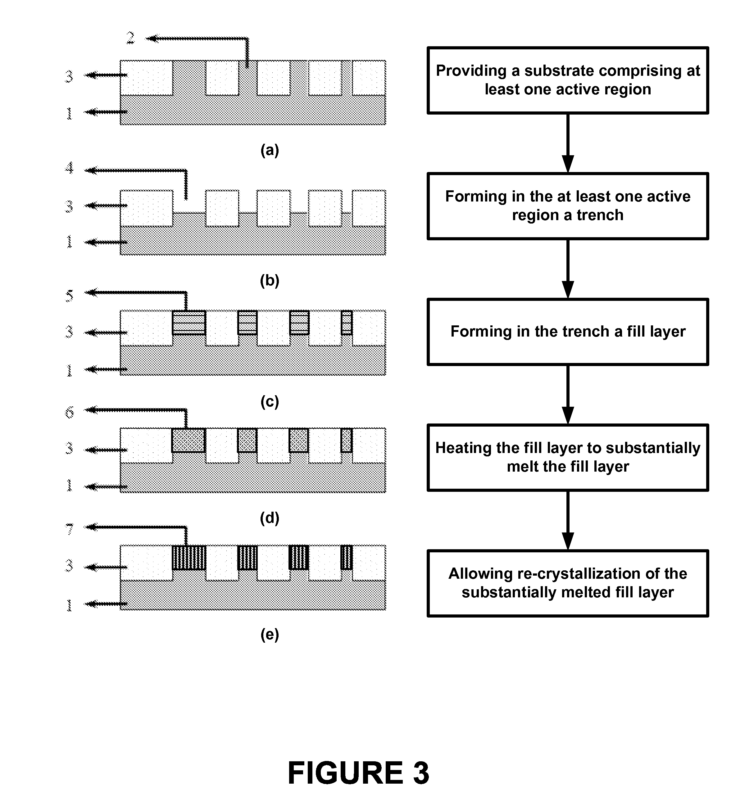
[0034]In the context of the present invention, the term “mono-crystalline” is meant to designate single-crystalline form of a material. The terms “trench”, “active region” and “insulating region” are herewith meant to have their commonly accepted meaning in the art. More specifically, an active region or an active area is comprised or formed of a semiconductor material and designates the physical part of a substrate on / in which the corresponding devices (such as e.g. transistors, resistors and capacitors) which perform computing and storage operations are defined. An insulating (isolation) region / area or a field oxide area is comprised or formed of an insulator (dielectric material) and serves to electrically isolate two or more devices on the same substrate. A trench is meant to refer to a recessed area having a rectangular cross-section. By the expression “the semiconductor material is exposed at the bottom of the trench” it is meant herein that the bottom of the trench is compris...


PUM


Abstract

A method is presented for forming mono-crystalline germanium or silicon germanium in a trench. In an embodiment, the method comprises providing a substrate comprising at least one active region that is adjacent to two insulating regions, forming in the active region a trench having a width of less than 100 nm, and forming in the trench a fill layer at a temperature of less than 450° C. that comprises germanium or silicon germanium and substantially fills the trench. The method further comprises heating the fill layer to a temperature sufficient to substantially melt the fill layer and allowing re-crystallization of the substantially melted fill layer, thereby forming mono-crystalline germanium or silicon germanium in the trench. In an embodiment, the method further comprises forming a mono-crystalline germanium or silicon germanium fin by removing at least a portion of the insulating regions. The mono-crystalline fin may be comprised in a fin field-effect-transistor (finFET).

Description

CROSS-REFERENCE TO RELATED APPLICATIONS[0001]This application claims priority to European Patent Application No. 09173972.2 filed Oct. 23, 2009, the contents of which are incorporated by reference herein in their entirety.TECHNICAL FIELD OF THE INVENTION[0002]The present invention is related to the field of germanium or silicon germanium FinFET devices and methods for forming the same. More specifically, the invention relates to epitaxial growth of mono-crystalline germanium or silicon germanium in trenches provided in a substrate. In particular, the present invention is directed to an improved method of forming mono-crystalline germanium or silicon germanium fin structures on a substrate.BACKGROUND OF THE INVENTION[0003]The scaling down of planar bulk complementary metal-oxide-semiconductor (CMOS) devices has become a major challenge in the semiconductor industry. While the sizes of many devices has been reduced (and corresponding performances have been improved), device architectu...

Claims


Application Information

Patent Timeline
IPC IPC(8): H01L21/20
CPCH01L29/785H01L29/66795
Inventor VANDERVORST, WILFRIEDWANG, GANG
Owner INTERUNIVERSITAIR MICRO ELECTRONICS CENT (IMEC VZW)
Why Eureka
Try Eureka