
Light-receiving device and method of manufacturing the same

a light-receiving device and light-receiving technology, which is applied in the direction of solid-state devices, adhesive types, semiconductor devices, etc., can solve the problems of reducing the strength reducing the reliability of the device, and reducing the yield. , to achieve the effect of reducing foreign materials, reducing the undercut of the frame member, and improving light permeability

Inactive Publication Date: 2011-05-05
SUMITOMO BAKELITE CO LTD
View PDF3 Cites 6 Cited by
  • Summary
  • Abstract
  • Description
  • Claims
  • Application Information

AI Technical Summary

Benefits of technology

The present invention aims to improve the reliability of a light-receiving device by reducing the amount of foreign materials generated in the inner space of the hollow package and preventing undercut in the frame member. The invention proposes a frame member composed of a cured resin composition with an alkali-soluble resin, a photopolymerizable resin, and an inorganic filler of 9% or less by weight. The resin composition should have a moisture permeability of 12 or more and an elastic modulus of 100 Pa or more at 80 degrees C. after exposure. By using this resin composition, the invention aims to reduce the amount of inorganic filler in the frame member to minimize foreign materials and improve light transmission.

Problems solved by technology

The present inventors have, however, found that in the prior art described in the above reference, further improvement in device reliability is difficult due to (i) insufficient strength of the frame member and (ii) a residue in an inner space which leads to yield reduction.
First, the inventors' findings have shown that reduction in strength of the frame member is caused by undercut occurring in the frame member.
Furthermore, significant undercut led to difficulty in improvement in resolution.
The foreign materials adhere to the transparent substrate and the base substrate, leading to adverse affect to imaging properties and to reduction in a yield.

Method used


Image

  • Light-receiving device and method of manufacturing the same
  • Light-receiving device and method of manufacturing the same
  • Light-receiving device and method of manufacturing the same

Examples


example 1

[0122]1.Synthesis of an Alkali-Soluble Resin ((meth)acrylic-Modified bis-A Novolac Resin)

[0123]In a 2 liter flask, 500 g of a solution of a novolac type bisphenol-A resin (Phenolite LF-4871, manufactured by Dainippon Ink And Chemicals, Incorporated) in MEK (methyl ethyl ketone) (solid content: 60%) was placed, followed by adding 1.5 g of tributylamine as a catalyst and 0.15 g of hydroquinone as a polymerization inhibitor to heat at 100° C. To the mixture, 180.9 g of glycidyl methacrylate was added dropwise over 30 min, and the mixture was reacted with stirring at 100 degrees C. for 5 hours to give 74% methacryloyl-modified novolac type bisphenol-A resin MPN001 (methacryloyl modification rate: 50%, “Methacryl-modified bis-A novolac resin” in Tables 1 and 2) with a solid content of 74%.

2. Preparation of an Adhesive Varnish

[0124]15% by weight of trimethylolpropane trimethacrylate (manufactured by Kyoeisha Chemical Co., Ltd., Light-Ester TMP) as a photopolymerizable resin, 5% by weight ...

example 2

[0126]The procedures in Example 1 were conducted except a composition of an adhesive varnish of Example 1 was as described below. A content of trimethylolpropane trimethacrylate was 5% by weight and a content of the (meth) acrylic-modified bis-A novolac resin was 70% by weight as a solid.

example 3

[0127]The procedures in Example 1 were conducted except a composition of an adhesive varnish of Example 1 was as described below. A content of trimethylolpropane trimethacrylate was 25% by weight and a content of the (meth)acrylic-modified bis-A novolac resin was 50% by weight as a solid.


PUM

PropertyMeasurementUnit
elastic modulusaaaaaaaaaa
wavelengthaaaaaaaaaa

Abstract

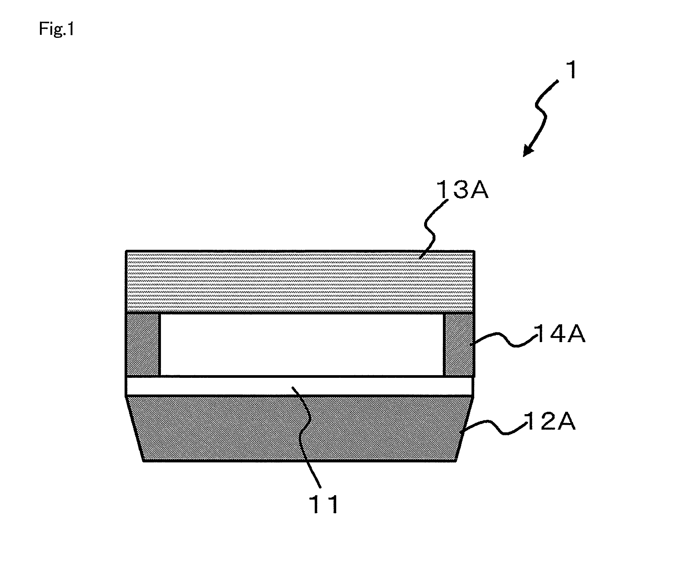
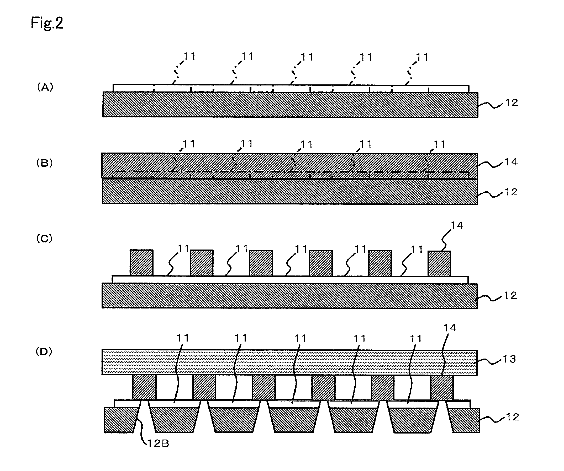
There is provided a device including at least one light-receiving unit 11, a base substrate 12A provided with the light-receiving unit 11, a transparent base substrate 13A disposed facing the base substrate 12A and the light-receiving unit 11, and a frame member 14A disposed around the light-receiving unit 11 between the base substrate 12A and the transparent substrate 13A. The frame member 14A consists of a cured resin composition. The resin composition contains an alkali-soluble resin, a photopolymerizable resin and an inorganic filler in 9% or less by weight. The photopolymerizable resin contains an acrylic polyfunctional monomer. The frame member 14A has a moisture permeability of 12 [g / m2·24 h] or more and an elastic modulus of 100 Pa or more at 80 degrees C.

Description

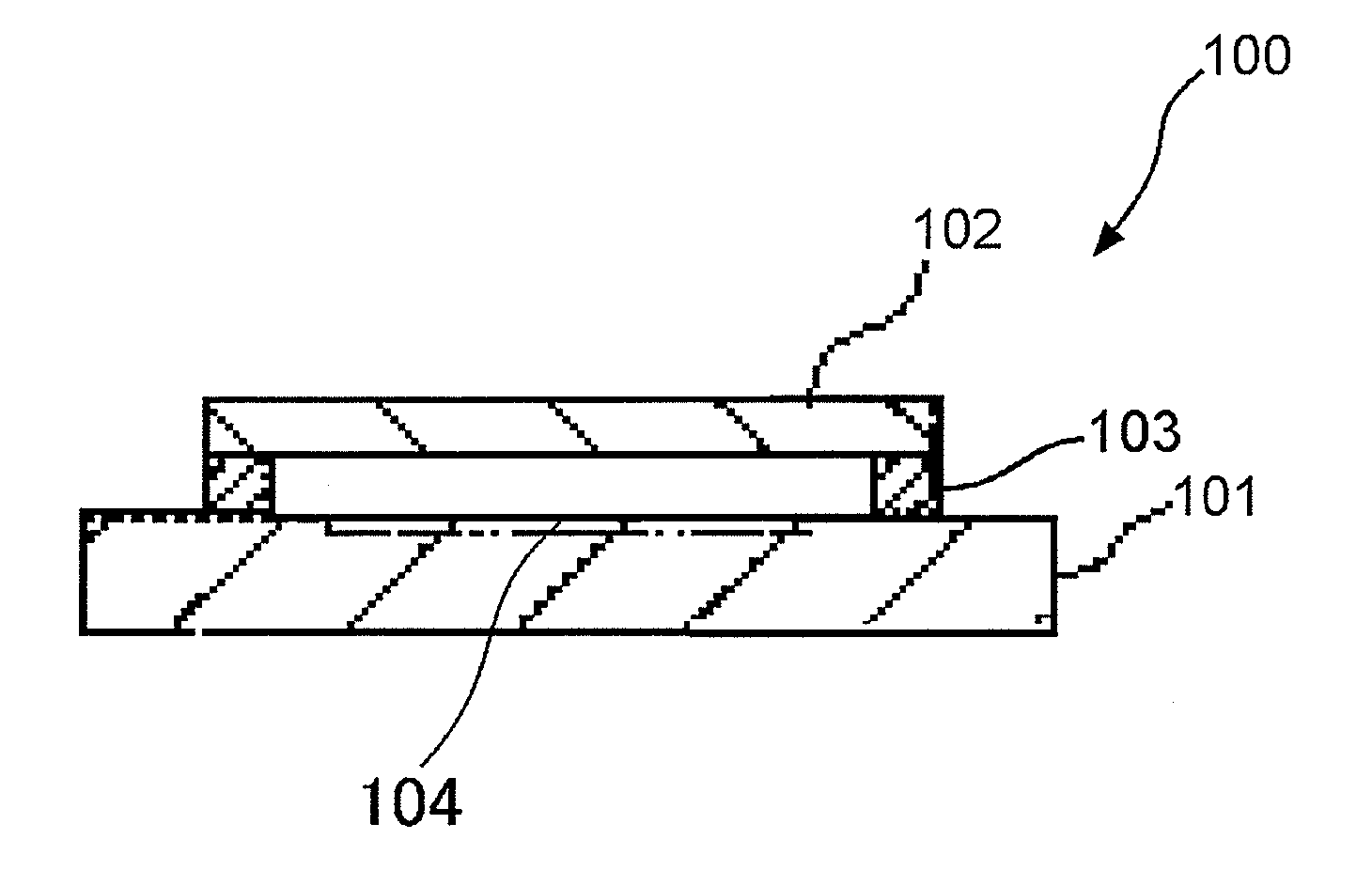
TECHNICAL FIELD[0001]The present invention relates to a light-receiving device and a method of manufacturing the same.BACKGROUND ART[0002]Conventionally, it is known that a solid-state image sensing device employing a hollow package as shown by FIG. 10. FIG. 10 is a cross-sectional view in a direction perpendicular to the substrate surface of a base substrate 101 and a transparent substrate 102. Such a solid-state image sensing device has abase substrate 101 on which a microlens array is formed, a transparent substrate 102, a light-receiving part 104 consisting of the microlens array and a frame member 103 formed around the light-receiving unit 104.[0003]As a process for such a solid-state image sensing device, photolithography technique such as exposure and development is used. Patent Document 1 shows an example of the technique. According to the technique of Patent Document 1, the frame member 103 consists of a resin composition containing a photocurable resin. Thus, depending on ...

Claims


Application Information

Patent Timeline
Patent Type & Authority Applications(United States)
IPC IPC(8): H01L31/0203H01L31/18
CPCC08L63/10C09J163/00H01L27/14618H01L31/0203C08L2666/22H01L2924/0002H01L2924/00
Inventor SHIRAISHI, FUMIHIROTAKAHASHI, TOYOSEISATO, TOSHIHIRO
Owner SUMITOMO BAKELITE CO LTD
Learn More