Method to Modify the Conductivity of Graphene

a graphene conductivity and conductivity technology, applied in solid-state devices, chemistry apparatus and processes, nanoinformatics, etc., can solve problems such as difficult application of dielectric materials to graphene, unsatisfactory current flow, and too thin dielectric layers, and achieve high contact resistance

Active Publication Date: 2011-05-12
GEORGIA TECH RES CORP
View PDF21 Cites 36 Cited by
  • Summary
  • Abstract
  • Description
  • Claims
  • Application Information

AI Technical Summary

Benefits of technology

[0012]In yet another aspect, the invention is a method of making a gated electrical device, in which a graphene structure is placed onto a non-conductive substrate. A metal gate is deposited directly on a portion of the graphene structure. The metal gate includes a first metal that has a high contact resistance with graphene. Two electrical contacts are deposited on the graphene structure so that the metal gate is disposed between the two electrical contacts.

Problems solved by technology

However, a dielectric layer that is too thin tends to leak and undesirable current flows from the metal layer to the graphene ribbon.
Applying a dielectric material to the graphene can be difficult because many dielectric materials do not adhere well to graphene.
However, such chemical modification can degrade the quality of the graphene.
Also, it is difficult to produce sufficiently thin dielectric layers on graphene using most conventional processes.

Method used


Image

  • Method to Modify the Conductivity of Graphene
  • Method to Modify the Conductivity of Graphene
  • Method to Modify the Conductivity of Graphene

Examples


Embodiment Construction

[0018]A preferred embodiment of the invention is now described in detail. Referring to the drawings, like numbers indicate like parts throughout the views. Unless otherwise specifically indicated in the disclosure that follows, the drawings are not necessarily drawn to scale. As used in the description herein and throughout the claims, the following terms take the meanings explicitly associated herein, unless the context clearly dictates otherwise: the meaning of “a,”“an,” and “the” includes plural reference, the meaning of “in” includes “in” and “on.” Methods of generating an patterning a graphene ribbon are disclosed in U.S. Pat. No. 7,015,142, issued to deHeer et al., which is hereby incorporated by reference.

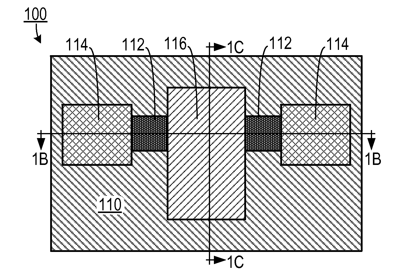
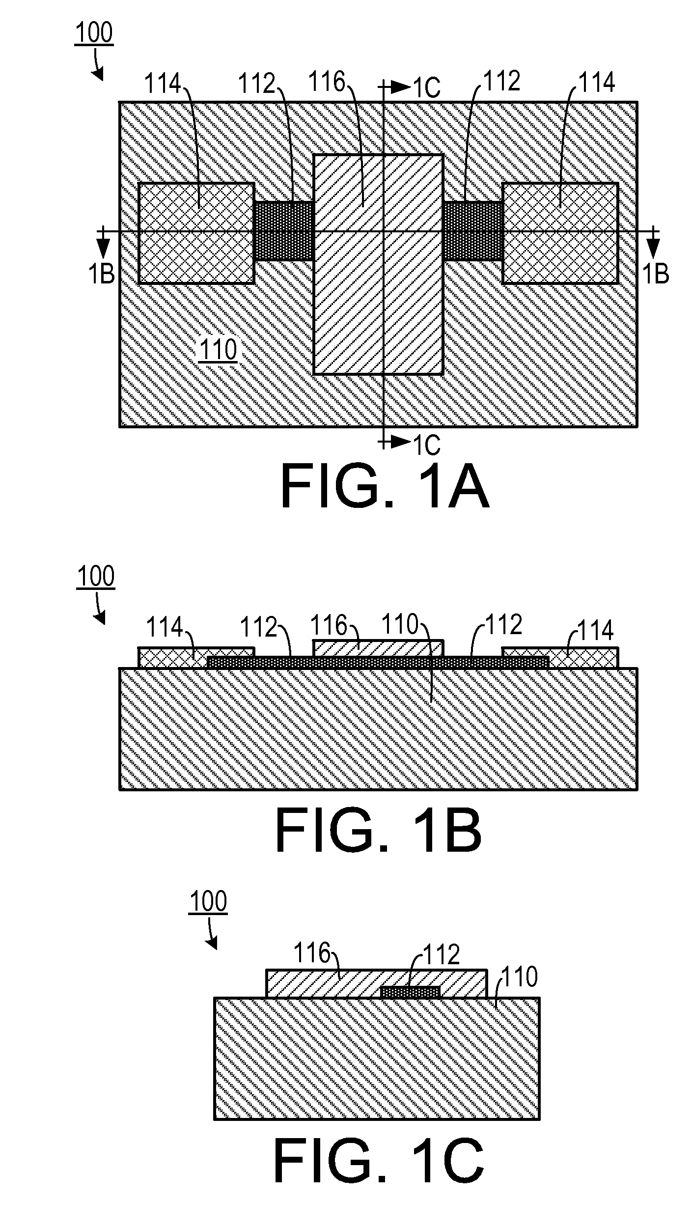
[0019]As shown in FIGS. 1A-1C, one embodiment of a gated electrical device 100, such as a field effect transistor, includes a non-conducting substrate 110, such as silicon oxide or silicon carbide. A graphene ribbon 112 (or other graphene structure) is disposed on the non-co...


PUM

PropertyMeasurementUnit
thickaaaaaaaaaa
non-conductiveaaaaaaaaaa
contact resistanceaaaaaaaaaa

Abstract

A gated electrical device includes a non-conductive substrate and a graphene structure disposed on the non-conductive substrate. A metal gate is disposed directly on a portion of the graphene structure. The metal gate includes a first metal that has a high contact resistance with graphene. Two electrical contacts are each placed on the graphene structure so that the metal gate is disposed between the two electrical contacts. In a method of making a gated electrical device, a graphene structure is placed onto a non-conductive substrate. A metal gate is deposited directly on a portion of the graphene structure. Two electrical contacts are deposited on the graphene structure so that the metal gate is disposed between the two electrical contacts.

Description

CROSS-REFERENCE TO RELATED APPLICATION(S)[0001]This application claims the benefit of U.S. Provisional Patent Application Ser. No. 61 / 250,722, filed Oct. 12, 2009, the entirety of which is hereby incorporated herein by reference.BACKGROUND OF THE INVENTION[0002]1. Field of the Invention[0003]The present invention relates to graphene devices and, more specifically, to a gated graphene device.[0004]2. Description of the Related Art[0005]Graphene has demonstrated numerous properties that make it suitable as a material for electronics. An important property of graphene is that its conductivity depends on the density of charge carriers (either electrons or holes) in the graphene. For example, when a voltage difference is applied between the ends of a graphene ribbon then a current will flow through the ribbon. The magnitude of the current depends on the density of the charge carriers in the graphene ribbon. This density can be modified using an electrostatic gate that selectively applies...

Claims


Application Information

Patent Timeline
Patent Type & Authority Applications(United States)
IPC IPC(8): H01L51/30H01L51/40
CPCB82Y10/00C01B2204/22H01L51/0558H01L51/0508H01L51/0045H10K85/20H10K10/46H10K10/484
Inventor DAVIDOVIC, DRAGOMIRDE HEER, WALTER A.MALEC, CHRISTOPHER E.
Owner GEORGIA TECH RES CORP
Why Eureka
Try Eureka