[0017]By providing an
antenna array according to an exemplary aspect of the invention it may be possible to provide a slanted polarization with bandwidth control wherein the array uses
diagonal modes instead of basic patch
modes. Furthermore, it may be possible to provide a small and compact
antenna array or antenna arrangement comprising a plurality of patch antenna elements which is mechanically less complex than known antenna arrays. Moreover, it may be possible to provide an antenna arrangement having similar performance for both polarization directions, e.g. for
horizontal and vertical polarization. Due to the less complex
assembly of an antenna arrangement according to an exemplary embodiment of the invention such an arrangement may be in particular suitable for simpler application like WLAN or
WiMAX applications. In addition it may be possible to achieve an antenna arrangement providing for a dual or
circular polarization. Circularly polarized antennas may be advantageous in further reducing the number of radios when dual-polarizations are not needed. Furthermore, it may be possible to provide for narrow electromagnetic
radiation beams for receiving and wide beams for transmitting links.
[0027]According to another exemplary embodiment of the
patch antenna array the first, second and third patch antenna elements have the same shape. In particular, the shape may be rectangular, however the antenna elements may be mirrored with respect to the straight axis. Moreover, the shape or geometrical design may be optimized with respect to
cross polarization isolation, for example the shape may be adapted to result in high
cross polarization isolation. This may be done by reducing a
radiation patch dimension in the cross-
polarization plane.
[0035]Providing of parasitic elements may be a suitable way to control antenna
beamwidth. Such a control may be easily achievable when using an antenna array according to an exemplary embodiment of the invention since a
coupling in the array may be less strong and a high-performance dual-slant polarized antenna array may be possible.
[0040]Summarizing an exemplary aspect of the present invention may be seen in providing a compact dual-slant (±45°) polarized antenna array by
interleaving single-polarized antenna elements. Thus, there may be provided a polarization agile antenna which may not become too large to practical application since no separate antenna arrays for the two polarizations may be needed. The single-polarized antenna elements may be designed so that they have high cross-polarization isolation by geometrical design. The preferred way may be to reduce the radiating patch dimension in the cross-
polarization plane. This type of radiating patch may be ideally suited to slanted polarizations, and the elements can be placed close to each other.
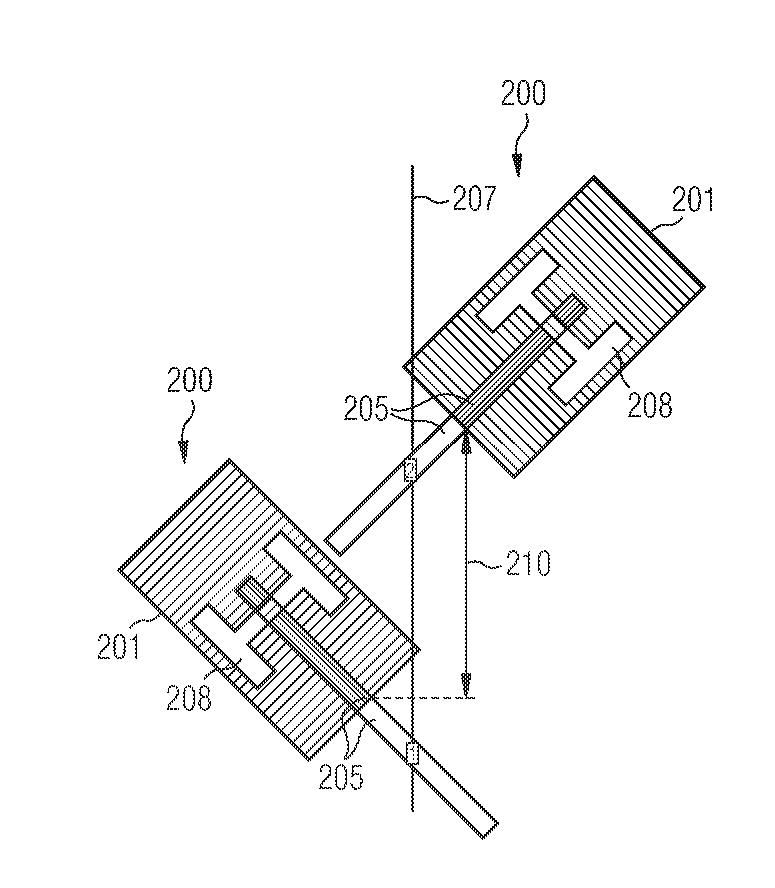
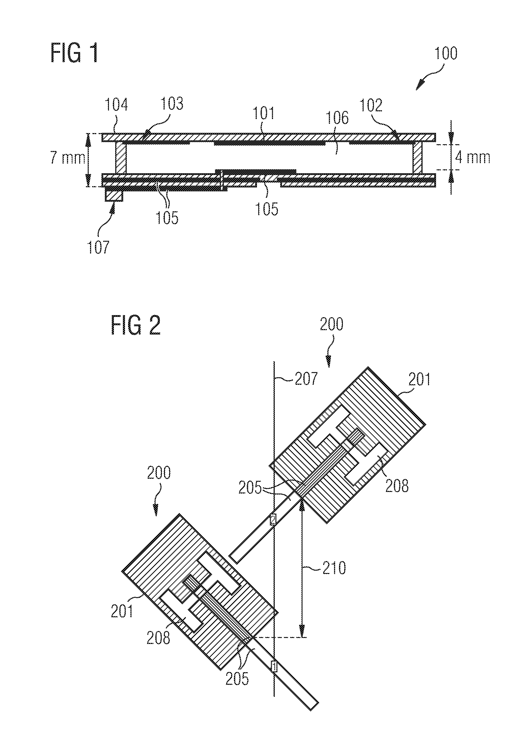
[0042]The antenna elements on both polarizations may be identical in construction and shape but are mirrored over the
vertical axis. The elements may be placed on a
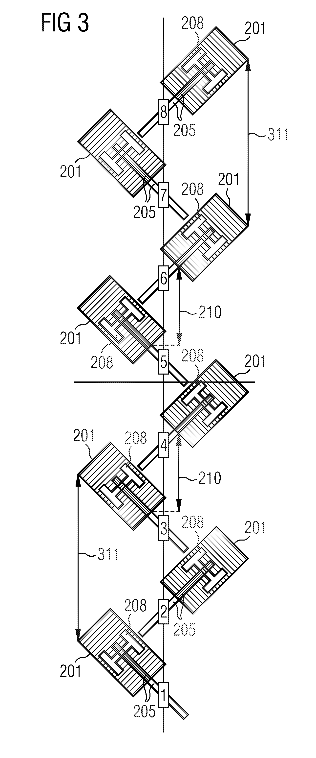
single line by stacking them in either vertical or horizontal direction. But, the most compact and good performing antenna may be achieved by offsetting the elements so that they are facing each other in the T-configuration mentioned above. FIG. 3, which will be described in detail afterwards, shows the vertically stacked variant of four such basic dual-polarization elements with an exemplary 0.6 λ0 displacement or separation. In practice, 0.5-0.7 λ0 displacement or separation may be optimal regarding
gain and sidelobe levels.
[0044]By providing a
patch antenna array or a patch antenna arrangement according to an exemplary aspect of the invention it may be possible that the basic
antenna design without parasitic patches may be applied to a low cost 5
sector antenna design having a good
electrical performance and very small
Printed Circuit Board (PCB) area. Furthermore, the antenna with parasitic patches may have very wide angular coverage for three sector designs. Moreover, the radiated beams from the wide
sector antenna may be much more symmetrical than obtainable with a dual-polarized single-element antenna with similar bandwidth according to the prior art. Additionally, symmetrical patterns may enable the use of
circular polarization, which may not be possible with a
broadband single-element antenna according to the prior art. In addition
circular polarization may be used to reduce the number of radios in a lower cost access point. The new antenna may virtually be the same size as a regular dual-polarized patch antenna, and may be used to
upgrade existing access point designs.

