Uniwafer thermoelectric modules

a technology of thermoelectric modules and thermoelectric modules, which is applied in the manufacture/treatment of thermoelectric devices, electrical devices, semiconductor devices, etc., can solve the problems of limited commercial application of thermoelectric devices, prohibitively high cost of thermoelectric devices, and poor cost performance of these devices, so as to enhance the thermoelectric figure of merit, simplify the process, and low cost

Inactive Publication Date: 2011-05-19
SYNERGY THERMOGEN INC +1
View PDF52 Cites 41 Cited by
  • Summary
  • Abstract
  • Description
  • Claims
  • Application Information

AI Technical Summary

Benefits of technology

[0014]Depending on certain embodiments, one or more benefits can be achieved with the uniwafer thermoelectric device. Advantages of the present invention over conventional assembled thermoelectric device include permitting the uses of broad ranges of substrate materials for enhancing the thermoelectric figure of merit of the functionalized regions, and simplifying the processes for spatially arranging a plurality of thermoelectric elements and configuring both thermal and electric interconnects thereof. Additionally, advantages lie in the utilization of well established semiconductor wafer processing technologies and low cost manufacturing foundries to substantially reduce the cost of the thermoelectric devices. These and other benefits will be described in more detailed throughout the present specification and particularly below.

Problems solved by technology

To date, thermoelectrics have had limited commercial applicability due to the poor cost performance of these devices compared to other technologies that accomplish similar means of energy generation or refrigeration.
Where there are no other technologies as suitable as thermoelectrics for lightweight and low footprint applications, thermoelectrics have nonetheless been limited by their prohibitively high costs.
These materials pose difficulties in the creation of cost-effective thermoelectric systems because of the difficulty associated with the synthesis of these semiconductors and their subsequent manufacturing into thermoelectric modules, which includes soldering and adhering metal contact layers to the thermoelectric semiconductors.
Limited infrastructure exists to process materials of this nature in this fashion after decades of research and development, and fundamental limits on their scalability can also limit the growth of this infrastructure.
However, their applicability has been limited due to the above considerations.
Costs associated with the processing and assembly of materials such as Bi2Te3 and PbTe often limit the use of thermoelectrics in all but a handful of applications.

Method used


Image

  • Uniwafer thermoelectric modules
  • Uniwafer thermoelectric modules
  • Uniwafer thermoelectric modules

Examples


Embodiment Construction

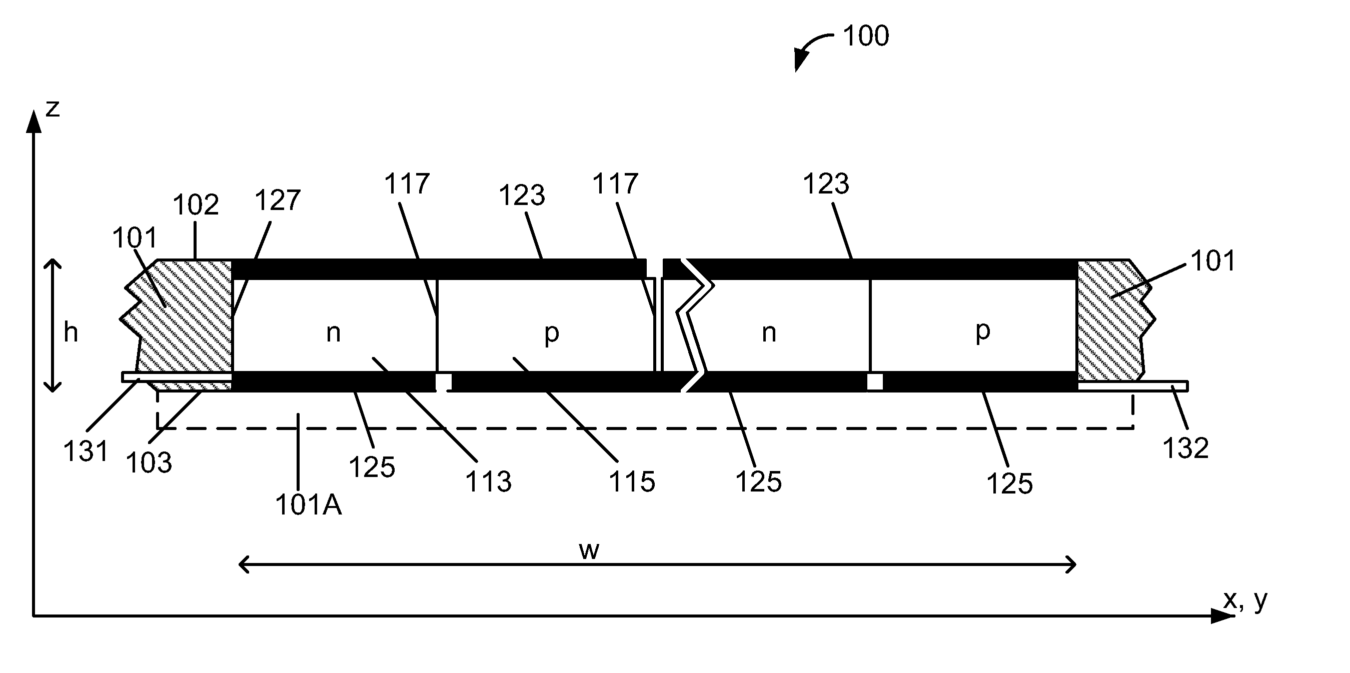
[0021]The present invention relates generally to thermoelectric devices. More particularly, the present invention provides a uniwafer thermoelectric device and a method for making the same. Merely by way of example, embodiments of the invention provide a method to achieve substantial reduction of process complexity, number of steps, and cost of thermoelectric module assembly that would entail the transformation of a single wafer of material into an entire thermoelectric device.

[0022]In accordance with certain embodiments of the present invention, one method to achieve reduction of the complexity, number of steps, and cost of thermoelectric module assembly would entail the transformation of a single wafer of material into an entire thermoelectric device. For example, one such wafer this could be accomplished in is one made from silicon. We herein outline an exemplary method by which to achieve this basic structure in accordance with certain embodiments of the present invention.

[0023]...


PUM


Abstract

A uniwafer device for thermoelectric applications includes one or more first thermoelectric elements and one or more second thermoelectric elements comprising respectively a first and second patterned portion of a substrate material. Each first/second thermoelectric element is configured to be functionalized as an n-/p-type semiconductor with a thermoelectric figure of merit ZT greater than 0.2. The second patterned portion is separated from the first patterned portion by an intermediate region functionalized partially for thermal isolation and/or partially for electric interconnecting. The one or more first thermoelectric elements and the one or more second thermoelectric elements are spatially configured to allow formation of a first contact region and a second contact region respectively connecting to each of the one or more first thermoelectric elements and/or each of the one or more second thermoelectric elements to form a continuous electric circuit.

Description

CROSS-REFERENCES TO RELATED APPLICATIONS[0001]This application claims priority to U.S. Provisional Patent Application No. 61 / 261,174, filed Nov. 13, 2009, entitled “THERMOELECTRIC MODULES MADE FROM A SINGLE WAFER OF MATERIAL” by inventor Matthew L. Scullin, incorporated by reference herein for all purposes.BACKGROUND OF THE INVENTION[0002]The present invention relates generally to thermoelectric devices. More particularly, the present invention provides a uniwafer thermoelectric device and a method for making the same. Merely by way of example, embodiments of the invention provide a method to achieve substantial reduction of process complexity, number of steps, and cost of thermoelectric module assembly that would entail the transformation of a single wafer of material into an entire thermoelectric device, but it would be recognized that the invention may have other device configurations.[0003]Thermoelectric materials are ones that, in the solid state and with no moving parts, can, ...

Claims


Application Information

Patent Timeline
Patent Type & Authority Applications(United States)
IPC IPC(8): H01L35/30H01L21/329
CPCH01L35/34H01L27/16H10N19/00H10N10/01
Inventor SCULLIN, MATTHEW L.
Owner SYNERGY THERMOGEN INC
Why Eureka
Try Eureka