Probe, electronic device test apparatus, and method of producing the same

a technology of electronic devices and test apparatus, which is applied in the direction of electronic circuit testing, measurement devices, instruments, etc., can solve the problem of poor electrical contact liable to occur at the center part of the first anisotropic conductive rubber member, and achieve the effect of suppressing the occurrence of poor electrical conta

Inactive Publication Date: 2011-05-26
ADVANTEST CORP +1
View PDF9 Cites 13 Cited by
  • Summary
  • Abstract
  • Description
  • Claims
  • Application Information

AI Technical Summary

Benefits of technology

[0037]In the present invention, the second conductor parts are provided on the whole of the second anisotropic conductivity elastic member. Due to this, the first board is resistant to warping and the first anisotropic conductivity elastic member can be applied with pressure substantially evenly, so occurrence of poor electrical contact can be suppressed.

Problems solved by technology

However, in the above probe, the second conductor parts are unevenly distributed at the peripheral edges of the second anisotropic conductive rubber member.
Therefore, when a semiconductor wafer under test is pushed against the probe, the pushing force is applied to only the peripheral edges of the first board, so the first board is warped, the first anisotropic conductive rubber member is not evenly pressed, and poor electrical contact is liable to occur at the center part of the first anisotropic conductive rubber member.

Method used


Image

  • Probe, electronic device test apparatus, and method of producing the same
  • Probe, electronic device test apparatus, and method of producing the same
  • Probe, electronic device test apparatus, and method of producing the same

Examples


embodiments of invention

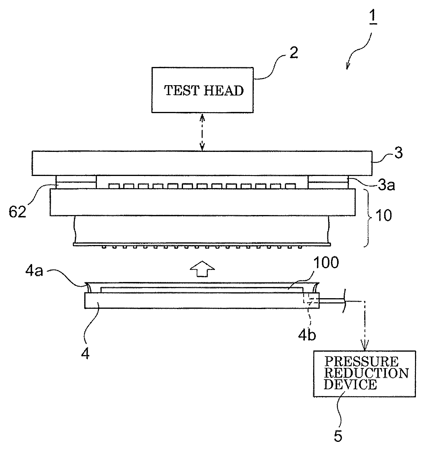
[0064]Below, an embodiment of the present invention will be explained based on the drawings. FIG. 1 is a schematic view showing an electronic device test apparatus in the present embodiment.

[0065]An electronic device test apparatus 1 in the present embodiment, as shown in FIG. 1, comprises a test head 2, a wafer mother board 3, a probe 10 (probe card), a wafer tray 4, and a pressure reduction device 5. At the time of testing IC devices, a semiconductor wafer under test 100 held on the wafer tray 4 is made to face the probe 10. In this state, the inside of a sealed space 80 (see FIG. 15) is reduced in pressure by the pressure reduction device 5. Due to this, the semiconductor wafer under test 100 is pushed against the probe 10 and electrical connection between component elements of the probe 10 is secured. Further, in this state, a tester (not shown) connected to the test head 2 inputs and receives test signals to and from IC devices built in the semiconductor wafer under test 100 so...


PUM


Abstract

A probe comprises: a membrane having a bump which contacts an input/output terminal of an IC device built into a semiconductor wafer under test; a pitch conversion board having a bottom surface on which a first terminal is provided and a top surface on which a second terminal connected to the first terminal is provided; a circuit board which is electrically connected to a test head and has a third terminal; a first anisotropic conductive rubber member having a first conductor part which electrically connects the bump of the membrane and the first terminal of the pitch conversion board; and a second anisotropic conductive rubber member having a second conductor part which electrically connects the second terminal of the pitch conversion board and the third terminal of the circuit board, and the second conductor parts are provided on the whole of the second anisotropic conductive rubber member.

Description

TECHNICAL FIELD[0001]The present invention relates to a probe for establishing electrical connection between a test apparatus main body and an IC device in an electronic device test apparatus for testing electrical characteristics of integrated circuit devices and other various types of electronic devices (hereinafter also referred to representatively as “IC devices”) built into a semiconductor wafer under test, an electronic device test apparatus comprising the same, and a method of production of the probe.BACKGROUND ART[0002]A large number of semiconductor integrated circuit devices are built into a silicon wafer or other semiconductor wafer, then are diced, wire bonded, packaged, and otherwise processed to form completed electronic devices. Such IC devices are tested for operation before shipment. The operating tests are run in the wafer state or state of the completed devices.[0003]As the probes used for testing IC devices in the wafer state, known in the past have been ones whi...

Claims


Application Information

Patent Timeline
Patent Type & Authority Applications(United States)
IPC IPC(8): G01R31/20
CPCG01R1/0735G01R3/00G01R1/07378
Inventor UMEMURA, YOSHIHARU
Owner ADVANTEST CORP
Why Eureka
Try Eureka