Semiconductor Element, Semiconductor Device, And Method For Manufacturing The Same

Inactive Publication Date: 2011-06-09
SEMICON ENERGY LAB CO LTD
View PDF99 Cites 116 Cited by
  • Summary
  • Abstract
  • Description
  • Claims
  • Application Information

AI Technical Summary

Benefits of technology

[0010]Miniaturizing a semiconductor element by reduction in channel length L of the semiconductor element is given as a way to increase the operation speed of

Problems solved by technology

However, reducing the space between the source electrode layer and the drain electrode layer through a

Method used


Image

  • Semiconductor Element, Semiconductor Device, And Method For Manufacturing The Same
  • Semiconductor Element, Semiconductor Device, And Method For Manufacturing The Same
  • Semiconductor Element, Semiconductor Device, And Method For Manufacturing The Same

Examples


Example

Embodiment 1

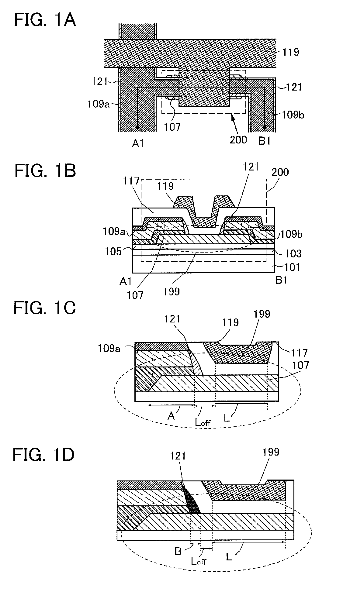
[0072]In this embodiment, an example of a cross-sectional structure of a semiconductor element according to one embodiment of the present invention will be described.

[0073]A semiconductor element of this embodiment will be described with reference to FIGS. 1A to 1D and FIGS. 28A and 28B. FIG. 1A is a top view of a semiconductor element of one embodiment of the present invention. FIG. 1B is a cross-sectional view taken along a line A1-B1 in FIG. 1A. FIGS. 1C and 1D are enlarged views of a dashed line portion 199 in FIG. 1B. In addition, FIGS. 28A and 28B each illustrate an example of a cross-sectional structure of a semiconductor element of one embodiment of the present invention. A transistor 200 illustrated in FIGS. 1A to 1D, a transistor 201 illustrated in FIG. 28A, and a transistor 300 illustrated in FIG. 28B are top-gate transistors.

[0074]The transistor 200 illustrated in FIGS. 1A and 1B includes a first insulating layer 103, a second insulating layer 105, an oxide s...

Example

Embodiment 2

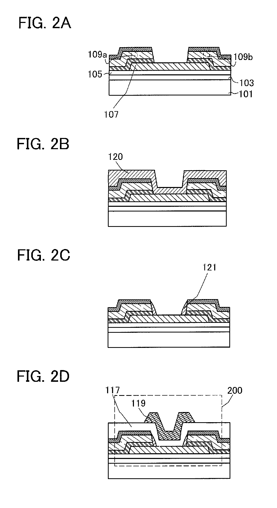
[0150]In this embodiment, an example of a method for manufacturing a semiconductor element will be described. One embodiment of a method for manufacturing a semiconductor element of this embodiment will be described with reference to FIGS. 2A to 2D.

[0151]A process of manufacturing the transistors 200 and 201, which are described in Embodiment 1, over the substrate 101 having an insulating surface will be described below.

[0152]Although there is no particular limitation on a substrate which can be used as the substrate 101 having an insulating surface, the substrate needs to have heat resistance high enough to withstand at least heat treatment performed later. For example, a glass substrate made of aluminosilicate glass, barium borosilicate glass, aluminoborosilicate glass, or the like can be used.

[0153]Note that a substrate formed of an insulator such as a ceramic substrate, a quartz substrate, or a sapphire substrate may be used instead of the glass substrate. Alternativ...

Example

Embodiment 3

[0224]In this embodiment, a method for manufacturing a transistor which is different from that described in the above embodiment will be described with reference to drawings. Note that the manufacturing process (a material and the like which can be used) described in this embodiment has a lot in common with that described in Embodiment 2. Therefore, in the following description, description of the same portions will not be given, and different points will be described in detail.

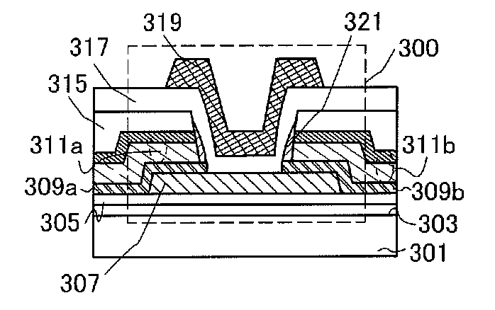
[0225]The transistor 300 illustrated in FIG. 28B includes the first insulating layer 303, the second insulating layer 305, the oxide semiconductor layer 307, the first source electrode layer 309a, the second source electrode layer 311a, the first drain electrode layer 309b, the second drain electrode layer 311b, the third insulating layer 315, the sidewalls 321, the gate insulating layer 317, and the gate electrode layer 319 over the substrate 301 having an insulating surface.

[0226]An example of a...


PUM


Abstract

The semiconductor element includes an oxide semiconductor layer on an insulating surface; a source electrode layer and a drain electrode layer over the oxide semiconductor layer; a gate insulating layer over the oxide semiconductor layer, the source electrode layer, and the drain electrode layer; and a gate electrode layer over the gate insulating layer. The source electrode layer and the drain electrode layer have sidewalls which are in contact with a top surface of the oxide semiconductor layer.

Description

TECHNICAL FIELD[0001]The present invention relates to a semiconductor element including an oxide semiconductor and a semiconductor device including the semiconductor element. The present invention relates to, for example, an electronic device including a semiconductor integrated circuit as a component. In addition, the present invention relates to a method for manufacturing the semiconductor element and the semiconductor device.[0002]In this specification, a “semiconductor device” refers to all devices which can function by utilizing semiconductor characteristics, and electro-optical devices, semiconductor circuits, electronic components, and electronic devices are all included in the category of the semiconductor device.BACKGROUND ART[0003]In recent years, semiconductor devices have been developed to be used as an LSI, a CPU, or a memory. A CPU is an aggregation of semiconductor elements each provided with an electrode which is a connection terminal, which includes a semiconductor ...

Claims


Application Information

Patent Timeline
IPC IPC(8): H01L29/786H01L21/336H01L21/44
CPCH01L27/1225H01L29/41733H01L29/7869H01L29/78648H01L29/66969H01L27/108H01L29/12H01L29/78696H01L29/42384H01L2029/42388H01L27/1255H10B12/00
Inventor SUZAWA, HIDEOMIKURATA, MOTOMUMIKAMI, MAYUMI
Owner SEMICON ENERGY LAB CO LTD
Why Eureka
Try Eureka