Semiconductor dice transfer-enabling apparatus and method for manufacturing transfer-enabling apparatus

a technology of transferenabling apparatus and semiconductor dice, which is applied in the direction of electrical apparatus, metal working apparatus, and article delivery, etc., can solve the problems of high initial cost, high initial cost, and limit the minimum size of dice that can be economically generated from wafers, so as to reduce manufacturing complexity and cost, and increase epitaxial quality and yield

Inactive Publication Date: 2011-06-09
COOLEDGE LIGHTING
View PDF98 Cites 22 Cited by
  • Summary
  • Abstract
  • Description
  • Claims
  • Application Information

AI Technical Summary

Benefits of technology

[0008]The subject matter of the present invention provides such an innovation wherein growth of high quality and high performance GaN-based LEDs on a source substrate is achieved, while at the same time a transfer-enabling apparatus for easy and cost-effective transfer of the LED dice from the wafer to a target substrate and a method for manufacturing the transfer-enabling apparatus are provided.
[0012]The method reduces manufacturing complexity and cost, and at the same time increases epitaxial quality and yield. A particular advantage of the anchors is that they maintain the position and orientation of the semiconductor dice during transfer by the apparatus with subnanometer precision, thereby enabling a variety of transfer techniques that would not otherwise be possible.
[0013]The shape and depth of the trenches and the thickness of the epitaxial growth material are chosen to leave parts of the side walls of the substrate exposed, thus allowing the die release process to proceed from these surfaces. The shape and depth of the trenches and the thickness of the epitaxial growth material and any other additional material are also chosen to provide temporary anchoring of the semiconductor during the release process and to provide for easy semiconductor die transfer from the source substrate.

Problems solved by technology

Many LED light sources employ high-powered LEDs, which pose thermal management and other related problems.
Another drawback with state-of-the-art LED devices is their high initial cost.
This process limits the minimum size of the dice that can be economically generated from the wafers, as there needs to be a minimum spacing for the “streets” between the dice.
However, dice of this scale cannot be economically generated from a source wafer using conventional wafer dicing techniques.
It is also difficult to transfer small LED dice to a target substrate using conventional “pick-and-place” robotic handling systems, as the various electrostatic and van der Waal forces tend to cause the dice to adhere to the pickup tools.

Method used


Image

  • Semiconductor dice transfer-enabling apparatus and method for manufacturing transfer-enabling apparatus
  • Semiconductor dice transfer-enabling apparatus and method for manufacturing transfer-enabling apparatus
  • Semiconductor dice transfer-enabling apparatus and method for manufacturing transfer-enabling apparatus

Examples


first embodiment

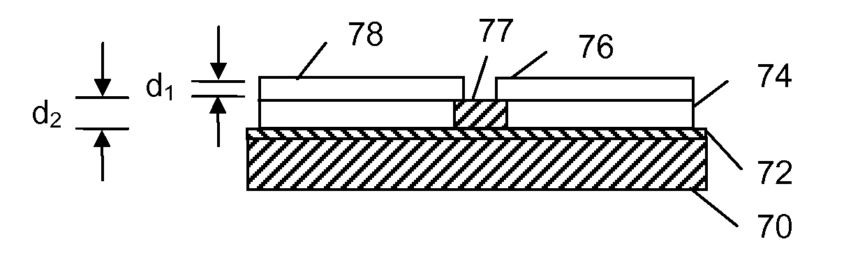
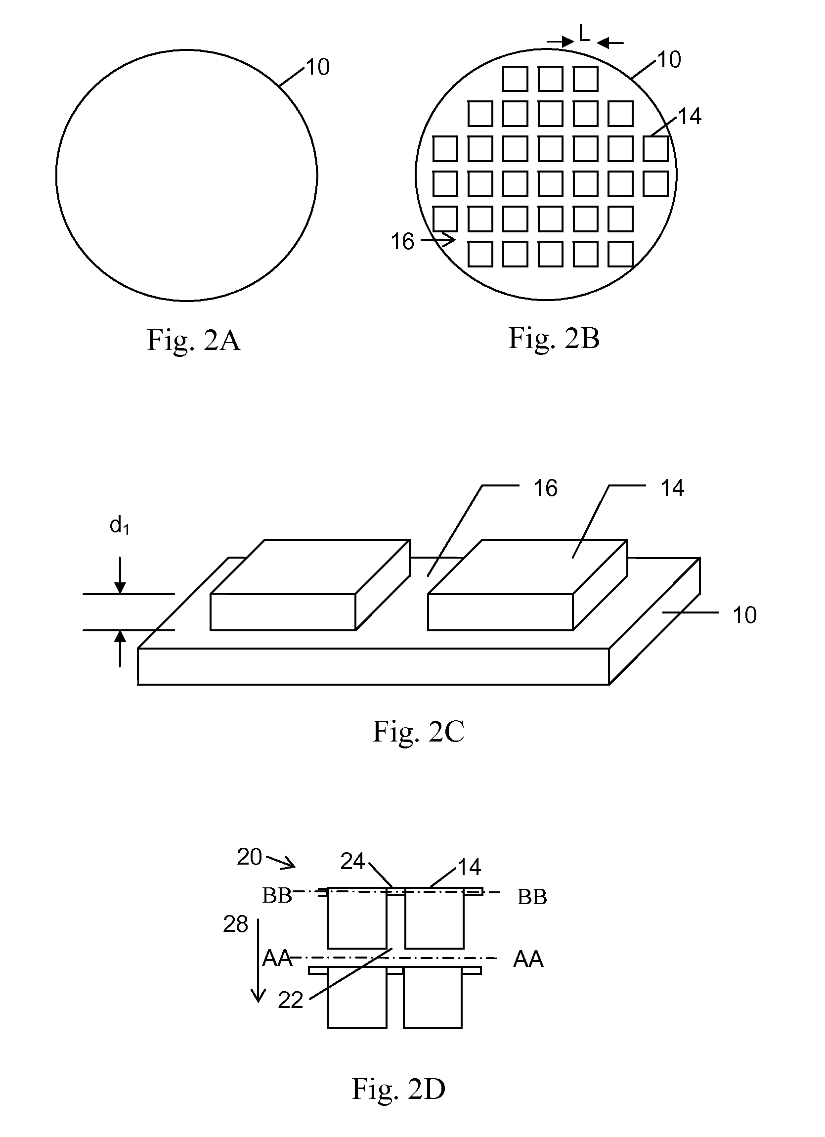
[0051]In a first embodiment, the epitaxial material is grown on Si(111) and the silicon substrate is etched making use of the preferential etching of Si on the Si(111) plane in the Si(110) direction in a potassium hydroxide (KOH) etch.

second embodiment

[0052]In a second embodiment, the epitaxial layer is grown directly on SiO2 or on SOI and the sacrificial oxide layer is removed in an isotropic etching process with BOE (buffered oxide etch) or hydrofluoric acid (HF).

third embodiment

[0053]In a third embodiment, a GaAs substrate is used and sacrificial layers include but are not limited to oxide layers, Al-rich AlGaAs layers, and AlAs layers that can be removed by a wet etching process. It is understood that the sacrificial layers and etch chemistries mentioned above are only examples and different sacrificial layers and etch chemistries can be selected.


PUM


Abstract

A transfer-enabling apparatus, produced by a method of manufacturing, includes a substrate patterned with islands separated by trenches and an epitaxial layer, grown at least on the islands, providing semiconductor dice in such a configuration partially released from said substrate and suspended over the substrate, and interconnected, by anchors of epitaxial or other material that are attached to the substrate. The anchors are of width less than or equal to than the semiconductor dice and define fracture zones at connections of the anchors with the semiconductor dice.

Description

[0001]This patent application claims the benefit of U.S. provisional application Nos. 61 / 285,134, 61 / 287,797 and 61 / 375,127, respectively filed Dec. 9, 2009, Dec. 18, 2009 and Aug. 19, 2010. The disclosures of said provisional applications are hereby incorporated herein by reference thereto.TECHNICAL FIELD[0002]The subject matter of the present invention is directed generally to the manufacture of transferable semiconductor dice and, more particularly, is concerned with a transfer-enabling apparatus providing semiconductor dice on a first substrate with anchors such that the dice can be transferred from the first substrate to a second substrate, and a method for manufacturing the transfer-enabling apparatus.BACKGROUND ART[0003]Illumination based on semiconductor light sources such as light-emitting diodes (LEDs) offers an efficient and long-lived alternative to fluorescent, high-intensity discharge, and incandescent lamps. Many LED light sources employ high-powered LEDs, which pose ...

Claims


Application Information

Patent Timeline
Patent Type & Authority Applications(United States)
IPC IPC(8): H01L21/78B26F3/00
CPCH01L25/0753H01L33/0095H01L33/0079H01L2224/83H01L2924/0002Y10T225/30H01L33/0093H01L2924/00
Inventor ASHDOWN, IANSPEIER, INGOSHEEN, CALVIN WADE
Owner COOLEDGE LIGHTING
Why Eureka
Try Eureka