Multi-layer micro structurefor sensing substance

a sensing substance and micro structure technology, applied in the field oframan scattering devices, can solve the problems of weak raman scattering signals in conventional raman spectroscopy for trace chemical detection, and achieve the effect of enhancing the intensity of scattered ligh

Inactive Publication Date: 2011-06-16
EXCELLENT CAPACITY LTD
View PDF8 Cites 29 Cited by
  • Summary
  • Abstract
  • Description
  • Claims
  • Application Information

AI Technical Summary

Benefits of technology

[0013]Embodiments may include one or more of the following advantages. The disclosed systems and methods may enhance the intensity of the scattered light for detecting trace chemicals. Different material compositions in the

Problems solved by technology

A limitation for conventional Raman spectroscopy is the w

Method used


Image

  • Multi-layer micro structurefor sensing substance
  • Multi-layer micro structurefor sensing substance
  • Multi-layer micro structurefor sensing substance

Examples


Embodiment Construction

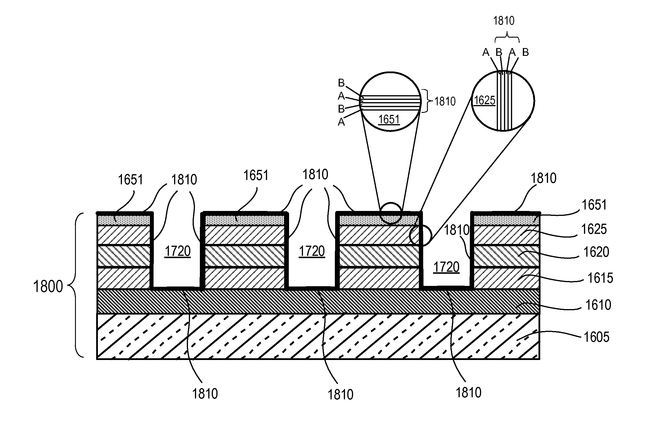
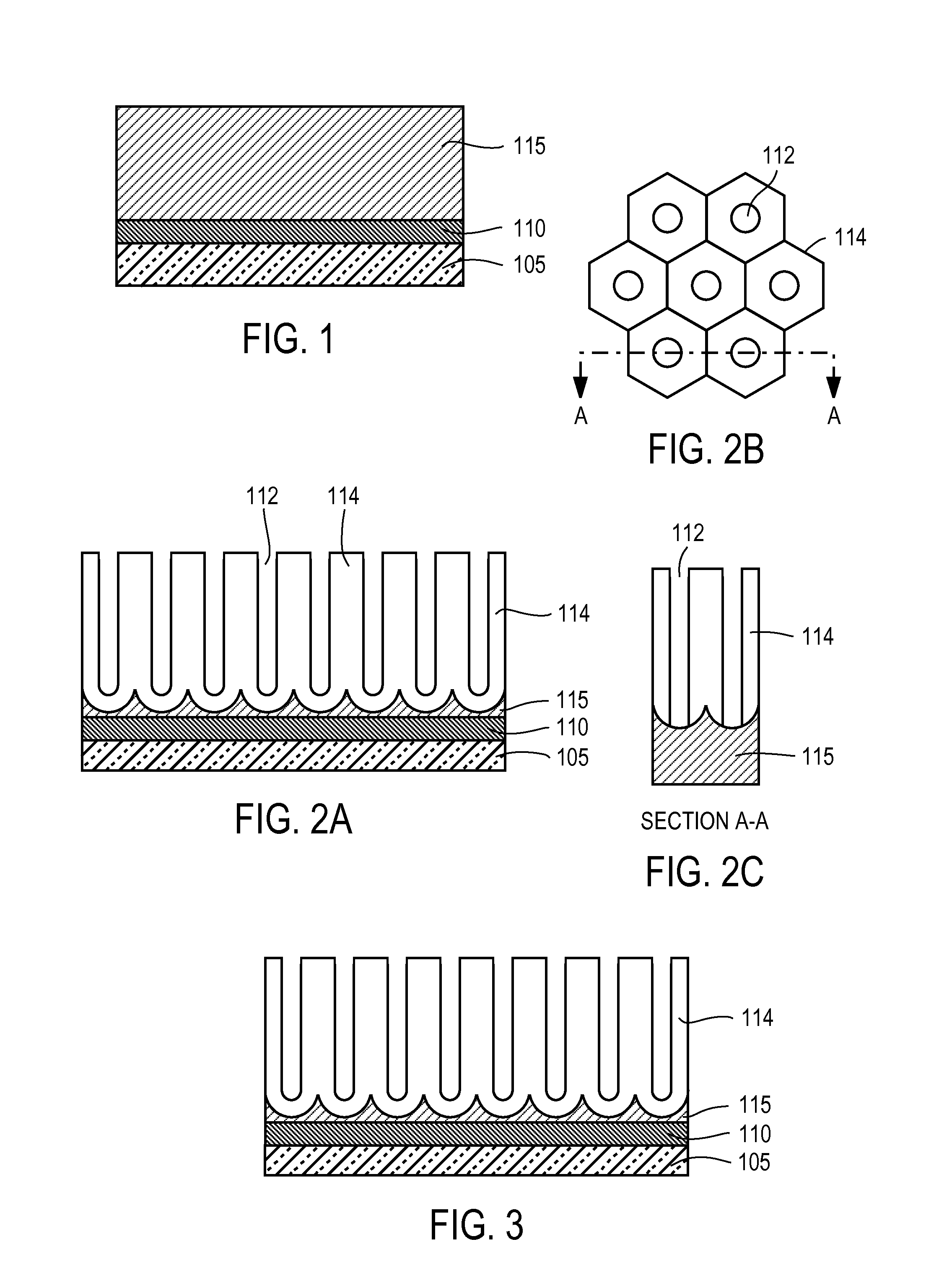
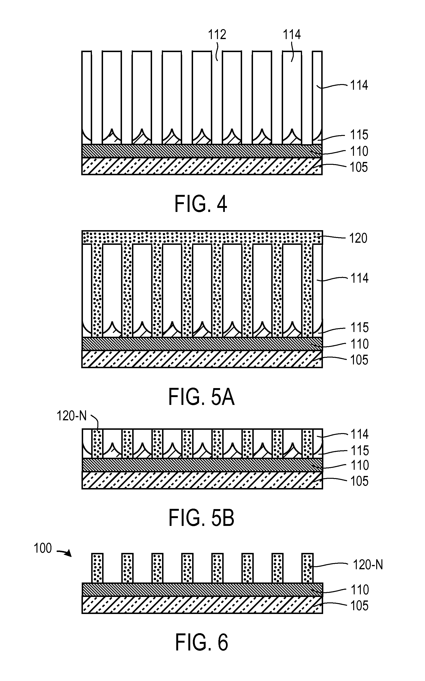
[0051]Referring to FIGS. 1 to 6 for a series of processing steps to fabricate a nano-structured noble metal surface of this application, FIG. 1 shows a two-layer structure with n-type (100) silicon wafer (3-8 Ω-cm) or oxidized (30-50 nm SiO2) p-type (100) silicon wafers (5-10 mΩ-cm), an electrically and thermally conductive layer 110 deposited on a (100) silicon substrate 105. The thickness of the conductive layer 110, such as Ti and Ni, is optimized to provide i) best adhesion to a subsequently deposited noble metal film, such as Ag, or Au film, etc., ii) electrical conductive film to apply electrical bias to sensing surface in field application, iii) thermal conductive layer to apply lower temperature of sensing surface, iv) thermal heat sink film to conduct localized heat generated by excitation of a light source. The thickness of this metal film is usually controlled in the range of 50 Å-50,000 Å, or 100 Å-1,000 Å. Then an aluminum layer 115 with purity of 99.999% and thickness ...


PUM


Abstract

A micro structure for sensing a substance using light scattering includes a substrate, a first layer on the substrate, wherein the first layer comprises a metallic material, a second layer over the first layer, and a mask layer over the second layer. A plurality of nano holes are formed through the mask layer and the second layer, wherein the plurality of holes are defined in part by internal surfaces on the second layer and the mask layer. Two or more structure layers are formed on the mask layer and the internal surfaces in the plurality of holes. The two or more structure layers comprise different material compositions.

Description

[0001]The present patent application is a Continuation-in-Part patent application of and claims priority to commonly assigned pending U.S. patent application Ser. No. 11 / 754,912, entitled “Light scattering device having multi-layer micro structure” filed May 29, 2007 by the same inventors, the content of which is incorporated herein by reference.BACKGROUND OF THE INVENTION[0002]The present application relates to Raman scattering devices including a sensing substrate having a micro structure.[0003]A limitation for conventional Raman spectroscopy is the weak Raman scattering signals for trace chemical detection. Techniques for increasing Raman scattering signals include Surface-Enhanced Raman Spectroscopy (SERS) and Surface-Enhanced Resonance Raman Spectroscopy (SERRS). Molecules of a trace chemical can be adsorbed on micro structural surfaces. It was discovered that noble metals on the surfaces of the micro structures could enhance the Raman scattering signal.[0004]There remains a ne...

Claims


Application Information

Patent Timeline
IPC IPC(8): H01L29/66H01L21/302
CPCG01N21/658
Inventor WANG, HONGLIU, ZHIMIN
Owner EXCELLENT CAPACITY LTD
Why Eureka
Try Eureka