Graphene structure, method for producing the same, electronic device element and electronic device

a graphene electrode and graphene technology, applied in the field of graphene structure, can solve the problems of increasing manufacturing cost, difficult to actually fix an intended amount of graphene at an intended position on a predetermined substrate, and difficult to patterned with high precision on a substrate, and achieve the effect of low cost and large area

Inactive Publication Date: 2011-06-16
EMPIRE TECH DEV LLC
View PDF1 Cites 89 Cited by
  • Summary
  • Abstract
  • Description
  • Claims
  • Application Information

AI Technical Summary

Benefits of technology

[0033]An electronic device element (including an electronic part element) and an electronic device according to the present disclosure includes a conductor or a semiconductor formed by a graphene structure in which graphene is disposed (fixed) on a substrate, and a bond is formed between a hydrophilized portion of the substrate and the graphene or between an unhydrophobized portion of the substrate and the graphene. Examples of the element or the device include transistors and solar cells ...

Problems solved by technology

However, it is significantly difficult to actually fix an intended amount of graphene at an intended position on a predetermined substrate, and it is a current state that the fixation of graphene is obliged to be performed by a follow-up method in which graphene flakes are fixed at unspecified positions on an adequate substrate, and then portions where the graphene flakes are resultantly arranged and fixed so as to be adequate in size, shape, and pattern are selected and applied to fabrication.
Since ...

Method used


Image

  • Graphene structure, method for producing the same, electronic device element and electronic device
  • Graphene structure, method for producing the same, electronic device element and electronic device
  • Graphene structure, method for producing the same, electronic device element and electronic device

Examples


Embodiment Construction

[0043]Embodiments of the present disclosure will be described with reference to drawings. In the drawings, the same elements are designated by the same reference numerals, and duplicated description is omitted. The positional relationship, such as left, right, top, and bottom, is based on the positional relationship shown in the drawing, unless specifically stated otherwise. The size ratios of the components are not limited to those illustrated in the drawings. Furthermore, the following embodiments are merely illustrative of the present disclosure, and the present disclosure is not limited to the embodiments. In addition, the present disclosure can be variously modified without departing from the spirit.

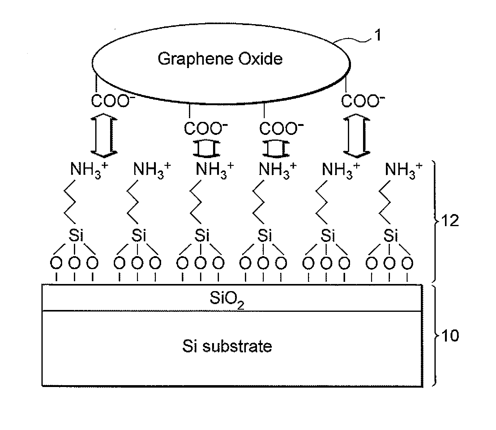
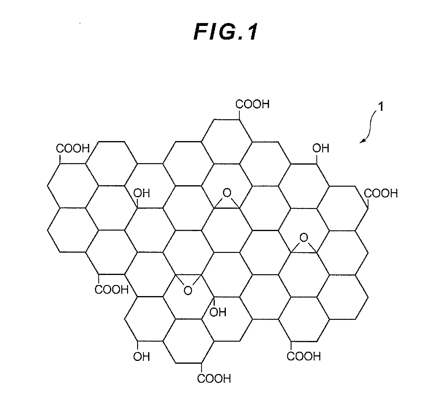
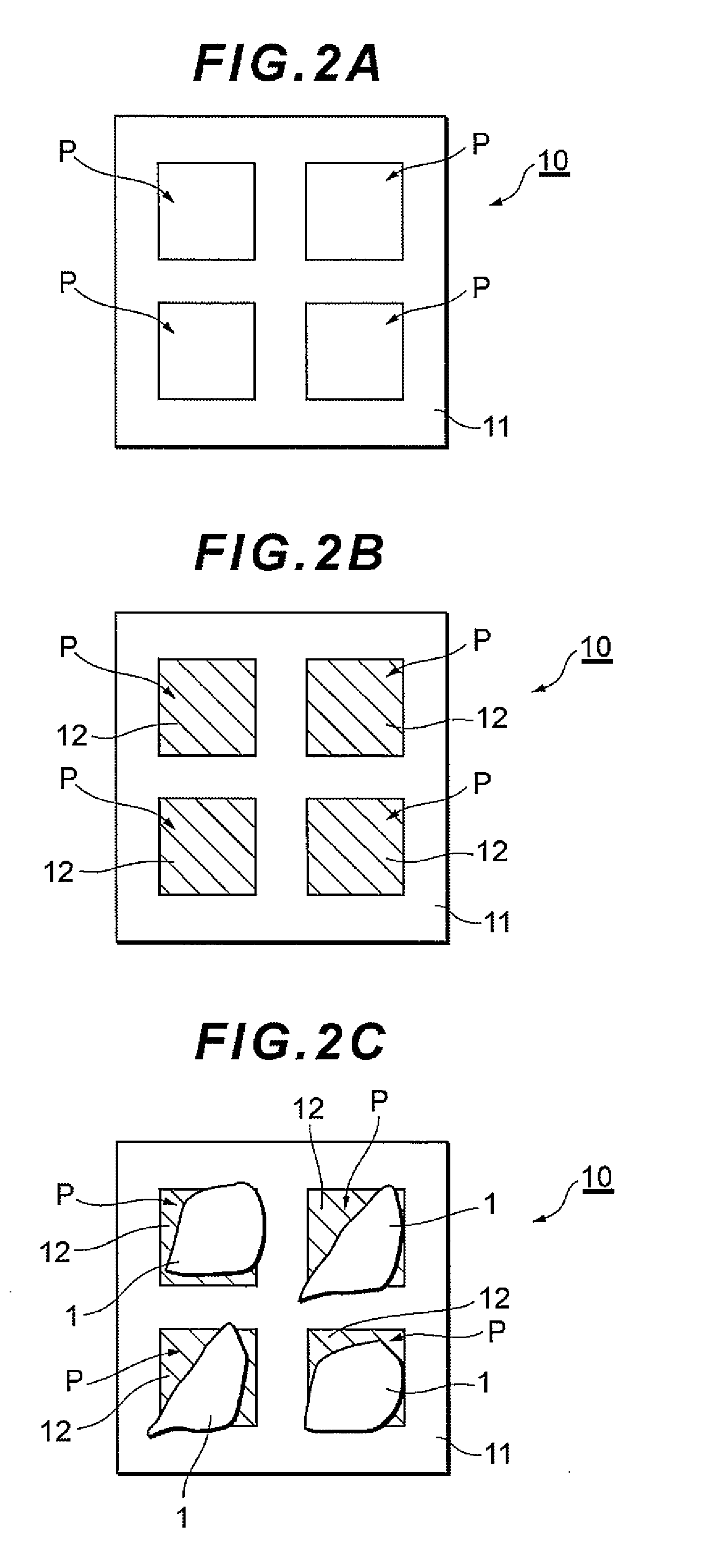
[0044]FIG. 1 is a plan view schematically showing a structure (molecular structure) of an oxide of graphene (graphene oxide: GO 1) used for producing a graphene structure according to the present disclosure.

[0045]The GO 1 can be produced (prepared) from natural graphite powder by a ...


PUM

PropertyMeasurementUnit
Hydrophilicityaaaaaaaaaa

Abstract

Provided are a graphene structure and a method for producing the same in which graphene can be patterned with high precision, and thereby microfabrication of electronic device elements and electronic devices using graphene is possible and the manufacturing cost can be notably reduced. A resist film is precisely patterned on a substrate, hydrophilized films are formed in openings of the resist film, and then GO is selectively fixed on the portions of the hydrophilized films by a chemical bond utilizing the hydrophilicity of the GO, and the GO is reduced to obtain a graphene structure in which graphene is selectively fixed to only the portions of the hydrophilized films. Thus, the graphene structure is constituted by disposing graphene on a substrate and forming a bond, by hydrophilization treatment, between the hydrophilized portion of the substrate and the graphene and/or between the unhydrophobized portion of the substrate and the graphene.

Description

CROSS REFERENCE TO RELATED APPLICATION[0001]This application claims the benefit of Japanese Application No. 2009-281897 filed on Dec. 11, 2009 which is incorporated herein by reference.BACKGROUND[0002]1. Technical Field[0003]The present disclosure relates to a graphene structure, a method for producing the same, a graphene electrode, an electronic device element (including a single element of an electronic part (component)), and an electronic device.[0004]2. Related Art[0005]Graphene, which composes a basic unit structure of graphite, allotropes such as carbon nanotube and carbon fullerene, other carbonaceous materials, and the like, is a single layer with a thickness of just one atom exfoliated from a layered structure of graphite, in other words, graphene has a hexagonal grid structure continuously formed by sp2-bonded carbon atoms in a sheet-like shape having a thickness of one atom. Thus, graphene consists of a single layer of carbon atoms and has a significantly thin thickness....

Claims


Application Information

Patent Timeline
IPC IPC(8): B32B3/10B32B9/00B05D5/12B05D3/04B05D5/00B05D3/10B05D1/36
CPCB82Y30/00B82Y40/00C01B31/0446C01B31/0476Y10T428/24802H01L31/022466H01L31/1884Y02E10/50Y10T428/30H01B1/04C01B32/184C01B32/192
Inventor SANDHU, ADARSH
Owner EMPIRE TECH DEV LLC
Why Eureka
Try Eureka