

Quantum Dot Photovoltaic Device and Manufacturing Method Thereof
- Summary
- Abstract
- Description
- Claims
- Application Information
AI Technical Summary
Benefits of technology
Problems solved by technology
Method used
Image

Examples
Embodiment Construction
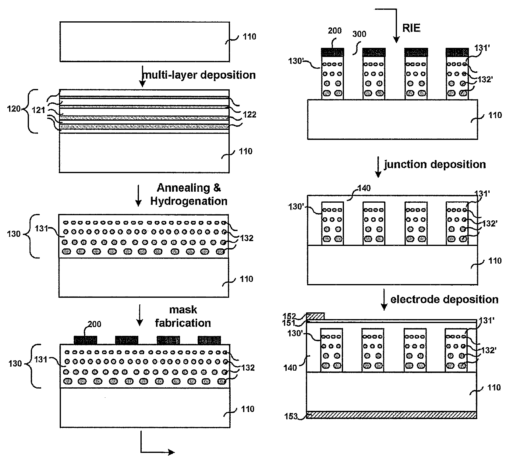
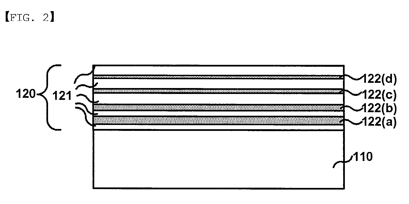
[0067]Hereinafter, a photovoltaic device and a manufacturing method thereof according to the present invention are specified with reference to the drawings. The following drawings are illustrated in order to sufficiently convey the spirit of the present invention to those skilled in the art. Thus, the present invention is not limited to the drawings below but may be embodied in another form. Furthermore, throughout the specification, the same reference numerals are used to refer to the same elements.
[0068]The technical and scientific terms used should be interpreted as having meanings typically understood by those skilled in the art unless otherwise definitions. Moreover, descriptions of known functions and constructions, even if they are pertinent to the present invention, are regarded as unnecessary and may be omitted when they would make the characteristics of the invention unclear.
[0069]Below the present invention is described based on the drawings that illustrate a p-type semic...
PUM
 Abstract
Description
Claims
Application Information