
Quantum dot photovoltaic device and manufacturing method thereof

a photovoltaic device and quantum dot technology, applied in the direction of semiconductor/solid-state device manufacturing, semiconductor devices, semiconductor devices, etc., can solve the problems of reducing the electric field, reducing the efficiency of devices, and increasing the distance between opposite electrodes of junctions, so as to achieve high-efficiency photovoltaic and high-efficiency photovoltaic. , the effect of favorable manufacturing

Active Publication Date: 2013-12-10
KOREA RES INST OF STANDARDS & SCI
View PDF8 Cites 3 Cited by
  • Summary
  • Abstract
  • Description
  • Claims
  • Application Information

AI Technical Summary

Benefits of technology

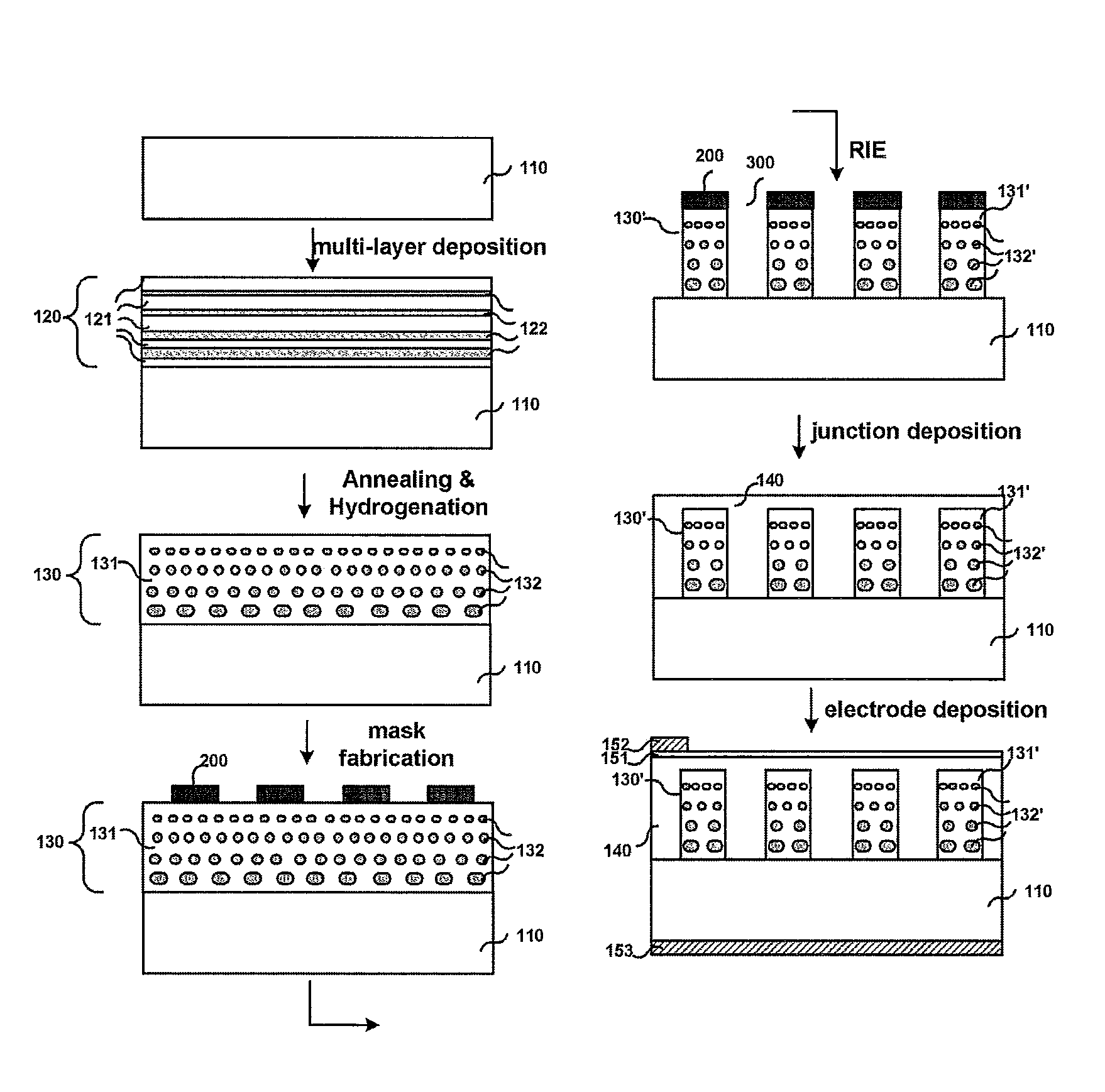
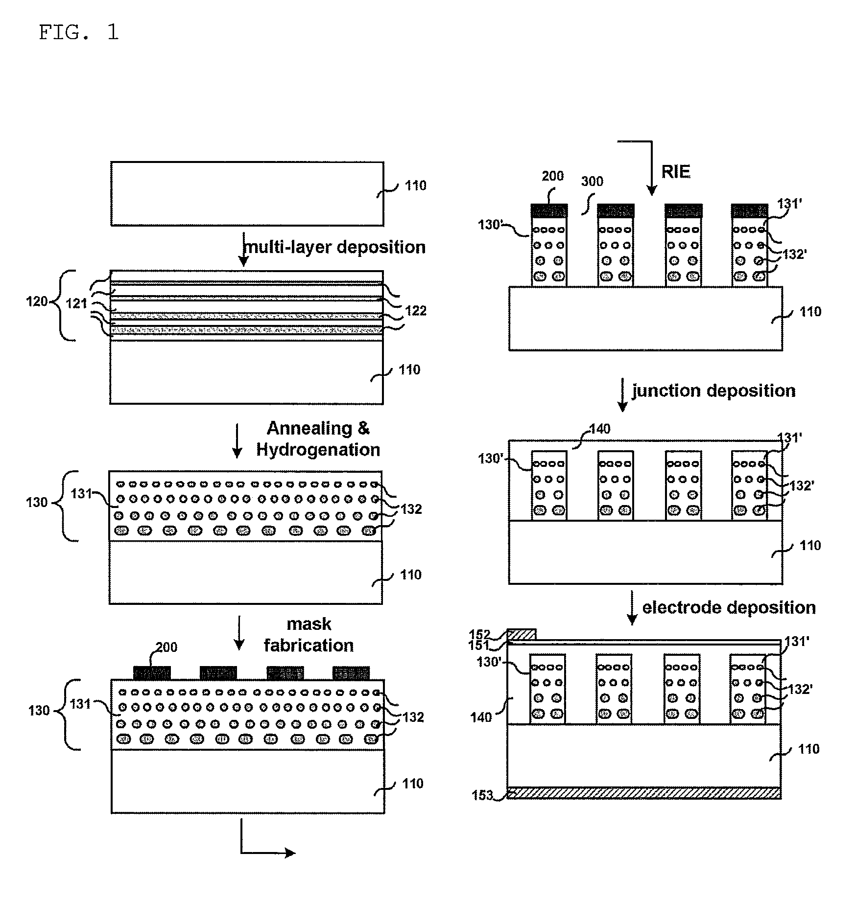
The present invention provides a photovoltaic device with semiconductor quantum dots incorporated in the p layer or n layer, which can absorb light over a wide wavelength range. The device has a low-dimensional nanostructure with a large-area vertical and radial junction structure, maximizing the contact area between the light absorbing layer and the p layer / n layer, and even if there are many defects as in amorphous silicon, electrons-holes can be effectively separated by the drift in an electric field, resulting in a high-efficiency photovoltaic device. The manufacturing method of the photovoltaic device is advantageous in that it is a low-dimensional nanostructure in a top-down manner without the use of a highly advanced lithographic or epitaxial process, and can be favorably manufactured using simple and easy procedures including deposition, annealing, etching and deposition, with easily controlling the size, position, and density of the semiconductor quantum dots.

Problems solved by technology

However, because of the properties of the photovoltaic devices that use the semiconductor principle, these devices have much lower efficiency and a shorter lifespan due to degradation, compared to silicon based photovoltaic devices, and thus the actual market occupation rate thereof is as low as about 3%.
In the conventional horizontal junction photovoltaic device, when the light absorbing layer (the p-n depletion layer, or the i layer) is formed thick, a large amount of light may be absorbed, but the distance between opposite electrodes of the junction may increase, undesirably reducing the electric field, making it difficult to separate the electron-hole pairs.
Hence, limitations are imposed on increasing the thickness of the junction.

Method used


Image

  • Quantum dot photovoltaic device and manufacturing method thereof
  • Quantum dot photovoltaic device and manufacturing method thereof
  • Quantum dot photovoltaic device and manufacturing method thereof

Examples


Embodiment Construction

[0067]Hereinafter, a photovoltaic device and a manufacturing method thereof according to the present invention are specified with reference to the drawings. The following drawings are illustrated in order to sufficiently convey the spirit of the present invention to those skilled in the art. Thus, the present invention is not limited to the drawings below but may be embodied in another form. Furthermore, throughout the specification, the same reference numerals are used to refer to the same elements.

[0068]The technical and scientific terms used should be interpreted as having meanings typically understood by those skilled in the art unless otherwise definitions. Moreover, descriptions of known functions and constructions, even if they are pertinent to the present invention, are regarded as unnecessary and may be omitted when they would make the characteristics of the invention unclear.

[0069]Below the present invention is described based on the drawings that illustrate a p-type semic...


PUM


Abstract

The present invention provides a semiconductor based photovoltaic device and a manufacturing method thereof. The semiconductor based photovoltaic device is able to absorb light with a wide band wavelength, and has high photoelectric conversion efficiency since it has high electron-hole pair separation efficiency. More specifically, the method for manufacturing the photovoltaic device comprises the steps of: a) forming a thin semiconductor quantum dot film on a p or n-type semiconductor substrate, wherein the thin semiconductor quantum dot film includes semiconductor quantum dots inside a medium at which the same type of impurities as the semiconductor substrate are doped; b) forming a pore array through partial etching, wherein the pore array penetrates the thin semiconductor quantum dot film; c) depositing a semiconductor in which complementary impurities to the semiconductor substrate are doped on the thin semiconductor quantum dot film at which the pore array is formed; and d) forming sequentially a transparent conductive film and an upper electrode on the semiconductor in which the complementary impurities are doped and forming a lower electrode at a lower portion of the semiconductor substrate.

Description

TECHNICAL FIELD[0001]The present invention relates to a semiconductor based photovoltaic device, which enables the absorption of light over a wide wavelength range and has high electron-hole pair separation efficiency so that it exhibits high photoelectric conversion efficiency, and a manufacturing method thereof, and particularly to a high-efficiency semiconductor based photovoltaic cell in which semiconductor quantum dots are provided in the p layer or n layer and the p-n junction has a large-area vertical junction structure, and to a method of manufacturing the same.BACKGROUND ART[0002]Research into various materials used in photovoltaic devices in addition to silicon in order to reduce the manufacturing cost and increase the efficiency has been carried out. However, because of the properties of the photovoltaic devices that use the semiconductor principle, these devices have much lower efficiency and a shorter lifespan due to degradation, compared to silicon based photovoltaic d...

Claims


Application Information

Patent Timeline
Patent Type & Authority Patents(United States)
IPC IPC(8): H01L31/0264
CPCH01L31/035218H01L31/18Y02E10/50H01L31/04
Inventor KIM, KYUNG JOONGLEE, WOOKIM, YONG SUNGKIM, YOUNG HEONHONG, SEUNG HUIYUN, WAN SOOKANG, SANG WOO
Owner KOREA RES INST OF STANDARDS & SCI
Learn More