Ion Beam Generator, and Substrate Processing Apparatus and Production Method of Electronic Device Using The Ion Beam Generator

a technology which is applied in the field of ion beam generator and substrate processing apparatus and production method of electronic devices using ion beam generator, can solve the problems of increasing the number of apertures formed in the lead-out electrode, the inability to secure the distance from the lead-out electrode to the substrate, and the inability to uniformly incident ion beams on the substrate. achieve the effect of narrowing the pitch of apertures, increasing the size of the apparatus,

Active Publication Date: 2011-06-23
CANON ANELVA CORP
View PDF5 Cites 12 Cited by
  • Summary
  • Abstract
  • Description
  • Claims
  • Application Information

AI Technical Summary

Benefits of technology

[0018]In the ion beam generator of the present invention, the ion beam lead out from the lead-out electrode is deflected by the deflecting electrode, so that the route of the ion beam from the lead-out electrode to the substrate can be provided sufficiently. Therefore, the substrate can be processed by a uniform ion beam without increasing the number of apertures in the lead-out electrode, narrowing the pitch of apertures, or increasing the size of the apparatus.
[0019]The electronic device can be produced with a good yield by performing uniform etching by the ion beam generator of the present invention.

Problems solved by technology

The above-described prior art is the apparatus which enters obliquely the ion beam to the substrate, but since the size of the entire apparatus is restricted, the distance from the lead-out electrode to the substrate cannot be secured sufficiently.
In other words, there is a problem that the ion beam incident on the substrate cannot be made uniform sufficiently.
Therefore, the number of apertures formed in the lead-out electrode is increased and a pitch of apertures is narrowed to make the ion beam uniform, but it is still insufficient.

Method used


Image

  • Ion Beam Generator, and Substrate Processing Apparatus and Production Method of Electronic Device Using The Ion Beam Generator
  • Ion Beam Generator, and Substrate Processing Apparatus and Production Method of Electronic Device Using The Ion Beam Generator
  • Ion Beam Generator, and Substrate Processing Apparatus and Production Method of Electronic Device Using The Ion Beam Generator

Examples


Embodiment Construction

[0034]Embodiments of the present invention are described below with reference to the drawings but the present invention is not limited to the embodiments.

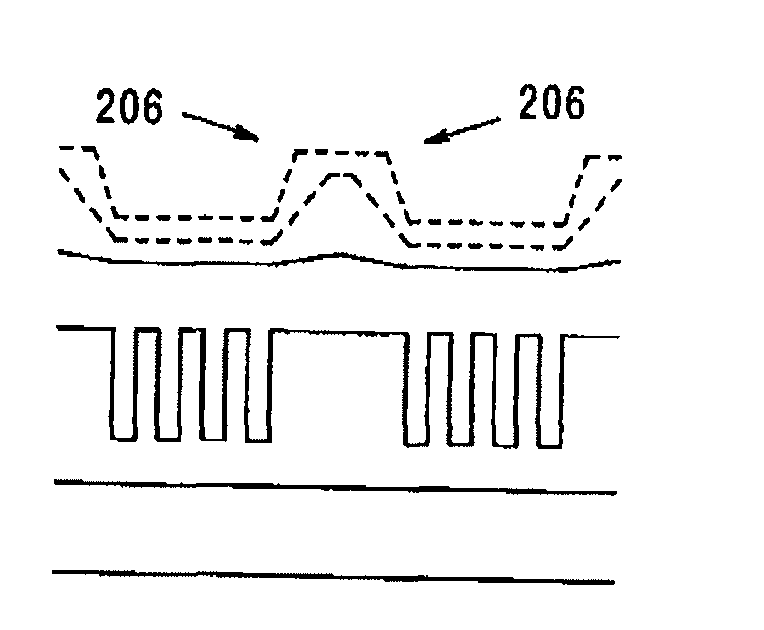
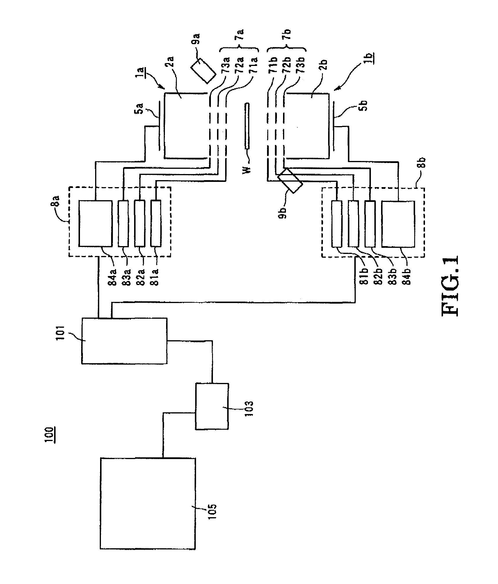
[0035]A substrate processing apparatus of the present invention is described below with reference to FIG. 1. FIG. 1 is a schematic view showing a structure of the apparatus of this embodiment viewed from above. As shown in FIG. 1, a substrate processing apparatus 100 is provided with a substrate (wafer) W, first and second ion beam generators 1a and 1b which are arranged to face each other with the substrate W between them, a control unit 101, a counter 103 and a computer interface 105.

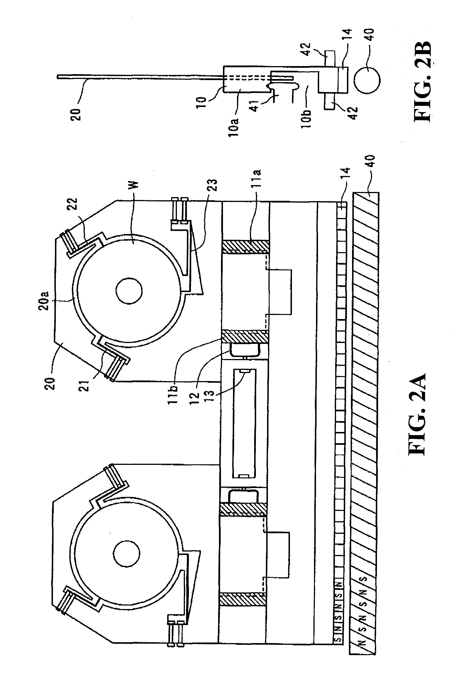
[0036]The substrate W of this embodiment is, for example, a substrate for a magnetic recording medium such as a hard disk and generally has an opening at the center of a substantially disk-shaped substrate. The substrate W is held in a posture erected in a vertical direction by, for example, a substrate carrier (conveying apparatus) shown in FIG. 2A ...


PUM

PropertyMeasurementUnit
pressureaaaaaaaaaa
pressureaaaaaaaaaa
pressureaaaaaaaaaa

Abstract

An ion beam generator generates plasma in a discharge tank 2, leads out an annular ion beam by a lead-out electrode 7, and deflects the ion beam in an annular center direction by a deflecting electrode 30 to enter a substrate W from the inclined direction to provide uniformity of the incident ion beam to the substrate without increasing the size of the whole apparatus.

Description

FIELD OF THE INVENTION [0001]The present invention relates to an ion beam generator for performing high-precision and uniform microfabrication and planarization processing of the surface for microfabrication of a semiconductor substrate and a magnetic disk substrate, a substrate processing apparatus using the above generator, and a production method of an electronic device by using the generator.BACKGROUND OF THE INVENTION[0002]A substrate processing apparatus provided with an ion beam generator is available as a technology for performing high-precision and uniform microfabrication and planarization processing of the surface for microfabrication of a semiconductor substrate and a magnetic disk substrate. JP-A S60-127732 discloses a semiconductor processing apparatus which has an accelerating grid disposed obliquely relative to the surface of a semiconductor in order to perform a high-precision surface processing. And, JP-A 2008-117753 discloses an ion gun that a lead-out electrode p...

Claims


Application Information

Patent Timeline
Patent Type & Authority Applications(United States)
IPC IPC(8): H01J27/00H01J37/147H01J3/28H01J37/305
CPCH01J27/024H01J37/30H01J2237/3151H01J2237/3142H01J2237/083
Inventor HIRAYANAGI, HIROHISAMIYOSHI, AYUMUABARRA, EINSTEIN NOEL
Owner CANON ANELVA CORP
Why Eureka
Try Eureka